Table of Contents
PCB Assembly DFM Checklist: Design Rules That Reduce Cost, Rework, and Lead Time
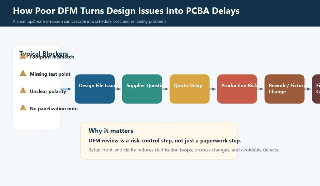
A PCB can look ready in CAD and still create trouble on the assembly floor. The Gerber files may export without errors. The BOM may look complete. The first prototype may even power on at an engineer’s bench. None of that proves the design is ready for stable PCB assembly.
Once a design reaches a PCBA factory, small decisions start to matter. A footprint mismatch, missing test point, unclear polarity mark, weak panelization plan, uncontrolled via-in-pad, or forgotten coating keep-out can slow down quotation, disrupt SMT programming, reduce solder yield, complicate fixture design, or increase rework.
That is the purpose of a PCB assembly DFM checklist. It gives engineers and purchasing teams a practical way to review the design before the RFQ becomes a production problem.
In delayed PCBA projects, the bottleneck is not always factory capacity. Quite often, the issue starts with files and assumptions: Gerber, BOM, centroid data, assembly drawings, test requirements, and process notes do not describe the same build condition. The factory then has to stop, ask questions, quote with assumptions, or redesign part of the production approach.
This guide combines DFM, DFA, and DFT into a single review flow for PCBA buyers. It focuses on the details that affect quotation speed, assembly yield, test coverage, cost stability, and the transition from prototype to pilot run and mass production.
Quick Answer: What Should Engineers Check Before Sending a PCBA RFQ?
Before sending a PCB assembly RFQ, check whether the design is manufacturable, assemblable, testable, and clearly documented. At a minimum, review file consistency, BOM-package matching, SMT spacing, polarity marks, fiducials, panelization, solder paste design, BGA/QFN risks, through-hole constraints, test points, programming access, special processes, and revision control.
| DFM Review Area | What to Check | Why It Matters |
|---|---|---|
| File completeness | Gerber or ODB++, drill files, BOM, centroid, assembly drawing, fabrication notes | Lets the supplier quote from a controlled file package instead of assumptions |
| Revision consistency | Gerber, BOM, centroid, drawings, firmware, and test files belong to the same revision | Prevents the supplier from quoting or building the wrong version |
| BOM-package matching | MPN, package, footprint, reference designator, DNP status, approved alternates | Reduces sourcing errors and footprint conflicts |
| SMT assembly | Fiducials, polarity, component spacing, paste layer, land patterns, tombstoning risk | Affects placement accuracy, solder yield, AOI, and rework |
| BGA/QFN/fine-pitch parts | Pad design, via-in-pad, thermal pad paste, X-ray access, rework clearance | Reduces hidden joint defects and process uncertainty |
| 0201/01005 passives | Pad symmetry, thermal balance, placement tolerance, stencil aperture control | Reduces tombstoning, skew, insufficient solder, and process variation |
| Through-hole and mixed assembly | Hole size, lead diameter, annular ring, connector support, wave/selective solder access | Affects solder fill, mechanical strength, labor, and fixture needs |
| Panelization | Rails, tooling holes, fiducials, V-cut, mouse bites, depanelization stress | Supports SMT handling and reduces board damage risk |
| DFT and test access | ICT/flying probe points, programming ports, FCT connectors, pass/fail criteria | Affects test coverage, fixture cost, and production debug speed |
| Special processes | Cleaning, conformal coating, potting, staking, labeling, serialization | Prevents late process conflicts and cost changes |
| Product context | Application environment, reliability target, volume, sourcing model, schedule | Helps the manufacturer recommend the right process and test strategy |
If the design uses BGA/QFN/fine-pitch parts, combines SMT and through-hole assembly, or targets industrial, medical, automotive-related, outdoor, power, or long-life applications, bring the PCBA manufacturer into the review before the layout is frozen. One early correction is usually far cheaper than a delayed build, fixture redesign, or production rework loop.
What Information Helps a Manufacturer Give Faster Feedback?
A manufacturer can estimate a simple board from limited files. A useful PCBA DFM review needs more than that. The supplier needs to understand what will be built and what the finished product must survive.
The most useful RFQ package answers two questions:
- What exactly should be built?
- What risks must the product survive in real use?
Application Environment and Reliability Level
Tell the supplier where the finished product will operate. A smart home controller, industrial control board, medical electronics module, outdoor IoT sensor, automotive-related assembly, and power electronics board do not carry the same manufacturing and reliability risks.
Useful context includes:
- indoor or outdoor use
- humidity, condensation, dust, salt spray, or chemical exposure
- vibration or repeated connector mating
- operating temperature range
- expected service life
- high-impedance, high-voltage, RF, sensor, or low-power circuit sensitivity
- required IPC class or customer acceptance standard, if applicable
- need for cleaning, conformal coating, potting, staking, or special packaging
Avoid vague phrases such as “standard quality” or “normal test.” They sound harmless, but they leave the supplier to decide what level of inspection, testing, and documentation is enough.
Production Stage and Volume Expectation
Prototype, pilot run, and mass production do not need the same review depth.
| Stage | DFM Focus |
|---|---|
| Prototype | File completeness, footprint match, first-build risks, basic assembly feasibility, early test access |
| Pilot run | Process window, yield data, test coverage, fixture readiness, packaging, traceability, revision control |
| Mass production | Repeatability, sourcing stability, takt time, MES records, inspection reports, change control |
If the current order is small but the product is expected to move into repeat production, say so in the RFQ. That information can change how the supplier thinks about panelization, test access, fixture investment, packaging, and traceability.
Test and Inspection Requirements
PCBA testing is not a single checkbox. AOI, X-ray, flying probe, ICT, programming, and FCT cover different risks.
Clarify:
- whether AOI is enough for the prototype
- whether BGA/QFN/X-ray inspection is required
- whether flying probe or ICT is expected
- whether FCT is needed
- how firmware should be loaded
- which interfaces must be tested
- whether test data should be recorded
- what pass/fail limits apply
If the layout does not support test access, the factory may still assemble the board. Debug, fault isolation, and production verification will simply become harder.
What DFM, DFA, and DFT Mean in PCB Assembly
DFM, DFA, and DFT are related, but they answer different engineering questions.
| Term | Full Meaning | Main Question |
|---|---|---|
| DFM | Design for Manufacturability | Can the PCB and assembly process be manufactured within normal factory capability and stable process control? |
| DFA | Design for Assembly | Can components be placed, soldered, inspected, handled, and reworked efficiently? |
| DFT | Design for Testability | Can the assembled board be programmed, tested, debugged, and verified in production? |
Many teams use “DFM” as a broad term for all three. That is fine in conversation. During engineering review, the distinction is useful because a board can pass one area and still fail another.
DFM: Manufacturing Feasibility
DFM checks whether the bare PCB and assembly process can be produced reliably.
Key areas include:
- board outline and size
- layer stackup
- copper weight
- trace and space capability
- drill size and aspect ratio
- annular ring
- impedance control
- surface finish
- solder mask registration
- paste layer
- via-in-pad control
- panelization
- process compatibility with the assembly line
For example, an RF or high-speed board may need controlled impedance stackup review before PCB fabrication. A board with small vias or high layer count may require closer fabrication capability confirmation. A board too small for stable handling may need panelization before it can move through SMT assembly.
DFA: Assembly Feasibility
DFA checks whether components can be assembled efficiently and consistently.
Important questions include:
- Are component footprints correct for the exact MPNs?
- Are component orientations clear?
- Is there enough spacing for placement nozzles, AOI, and rework?
- Are tall parts blocking smaller parts?
- Are connectors mechanically supported?
- Are through-hole parts compatible with wave, selective, or manual soldering?
- Are heat-sensitive parts placed away from high thermal stress zones?
- Can operators inspect and repair the assembly without damaging nearby components?
A PCB may be easy to fabricate and still be awkward to assemble. DFA is where those risks become visible.
DFT: Production Testability
DFT checks whether manufacturing defects and functional failures can be found quickly and repeatably.
Review:
- test point access for key nets
- power and ground access
- probe pad size and spacing
- programming connector or pad access
- fixture keep-outs
- FCT interface accessibility
- firmware version control
- pass/fail limits
- data logging and traceability requirements
If a product needs ICT or fixture-based testing, test access has to be designed into the layout. Adding good access after layout release is often difficult.
Why Poor DFM Causes Quote Delays, Rework, and Reliability Risk
DFM Issues Often Appear Before Production Starts
In quotation and engineering review, the same blockers appear again and again.
| Issue | Example | Why It Delays the Project |
|---|---|---|
| BOM and footprint mismatch | BOM specifies 0402, but PCB pads match 0201 | Supplier must confirm whether BOM or layout is correct |
| Wrong or incomplete centroid data | X/Y coordinates, side, rotation, or reference designators do not match PCB/BOM | SMT programming cannot proceed safely |
| Unclear polarity marks | Diodes, electrolytic capacitors, IC pin 1, LEDs, or connectors are unclear | First article inspection becomes slower and orientation errors become more likely |
| No panelization notes | Board is very small, narrow, or odd-shaped with no rail strategy | Supplier must redesign handling and assembly panel |
| Missing test requirements | RFQ says “functional test required” but gives no procedure | Fixture cost, labor, and lead time cannot be estimated |
| Coating or cleaning not mentioned | Special process appears after quote | Cost, sequence, masking, test order, and component compatibility may change |
A clean RFQ does not need to solve every manufacturing question before the supplier sees it. It should give the supplier enough information to ask the right questions quickly.
Small Design Problems Can Become Production Defects
Some DFM issues are easy to miss in layout review but serious once boards enter production.
| Design Problem | Possible Production Defect | Typical Prevention |
|---|---|---|
| Fine-pitch pads too close or paste aperture too large | Solder bridging | Review land pattern, solder mask, and stencil aperture |
| 0201/0402 pads thermally unbalanced | Tombstoning | Balance pad geometry and copper connection |
| QFN exposed pad paste not controlled | Floating package, voiding, insufficient thermal performance | Segment paste aperture and review thermal via design |
| Via-in-pad not filled or capped when needed | Solder wicking, weak BGA/QFN joints | Define filled/capped vias where required |
| Hole too small for through-hole lead | Poor insertion or poor solder fill | Match finished hole size to lead diameter and tolerance |
| Connector lacks mechanical support | Cracked solder joints under cable stress | Add support pins, mounting points, strain relief, or staking |
| Test points missing | Low ICT/flying-probe coverage | Plan DFT before layout release |
| Components too close to breakaway tabs | Solder joint or MLCC cracking during depanelization | Move sensitive parts away from tabs or change panel method |
DFM Is Risk Control, Not Only Cost Reduction
DFM can reduce PCB assembly cost, but cost is only part of the story. The deeper value is risk control.
For cost-sensitive consumer electronics, some tradeoffs may be reasonable. For industrial control, medical electronics, outdoor IoT, power electronics, automotive-related electronics, or long-life equipment, a small process weakness can become a field failure after humidity, vibration, temperature cycling, cable stress, or long operating time.
The question is not only:
Can this board be built once?
The better question is:
Can this board be built repeatedly, inspected consistently, tested effectively, and shipped with acceptable reliability for its real operating environment?
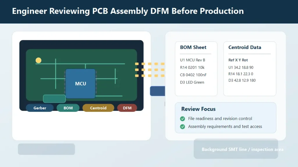
Files Needed for a Useful PCBA DFM Review
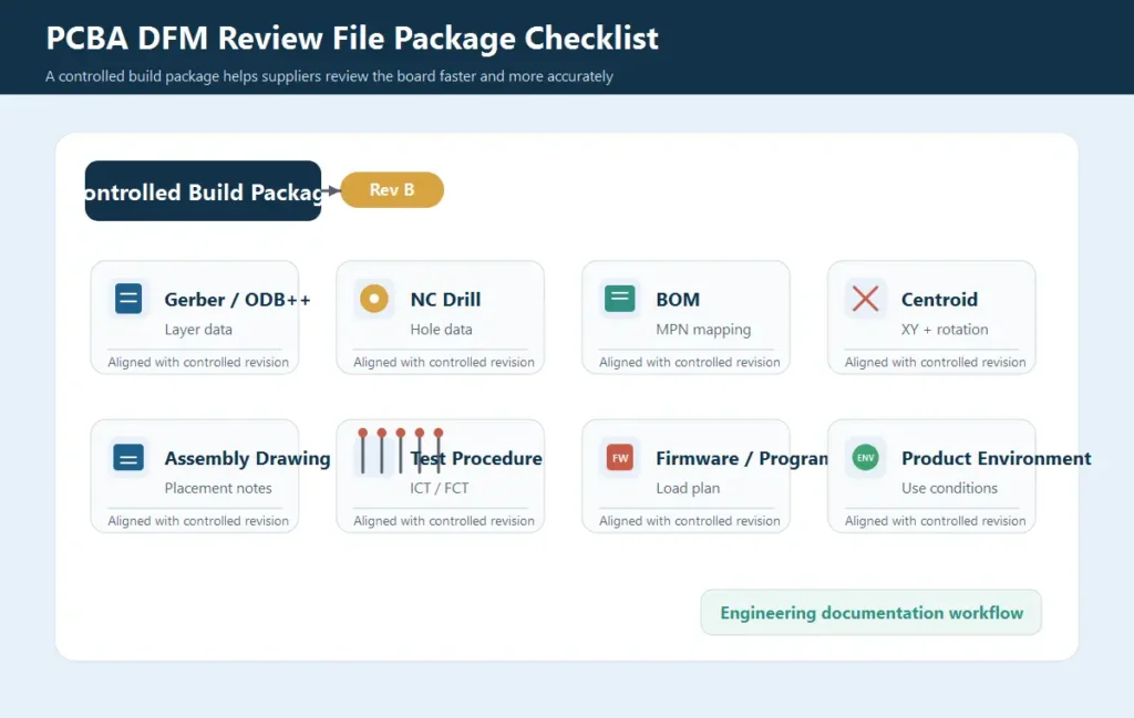
Gerber, ODB++, or IPC-2581 Files
These files define the PCB manufacturing data. The supplier reviews:
- copper layers
- solder mask layers
- silkscreen layers
- paste layers
- NC drill files
- board outline
- plated and non-plated holes
- stackup notes
- impedance requirements
- surface finish
- copper weight
- fabrication notes
- panelization data, if provided
Gerber is widely accepted for most projects. ODB++ or IPC-2581 can reduce ambiguity on more complex designs because more manufacturing information is packaged together. The file format matters less than the quality, completeness, and revision control of the data.
BOM and Approved Alternates
The BOM is the identity document for every component. It should include:
- reference designator
- quantity
- manufacturer name
- manufacturer part number
- package
- description
- value and tolerance where useful
- voltage/current/power rating where relevant
- DNP or DNI status
- approved alternates if allowed
- customer-supplied or supplier-sourced status
Common BOM problems include generic descriptions, missing MPNs, obsolete parts, wrong package, missing DNP notes, and unapproved substitutions.
For turnkey or partial turnkey PCBA projects, approved alternates are especially useful. They reduce shortage risk without giving the supplier uncontrolled freedom to substitute parts.
Centroid and Assembly Drawing
The centroid file, also called Pick-and-Place or XY data, tells SMT equipment where each component should be placed.
It should include:
- reference designator
- X coordinate
- Y coordinate
- rotation angle
- top or bottom side
- package or footprint reference where available
The assembly drawing helps engineers, operators, and inspectors interpret the machine data. It should show:
- component location
- pin 1
- polarity
- connector orientation
- DNP parts
- special assembly notes
- manual soldering notes
- coating or keep-out notes if applicable
Centroid, BOM, Gerber, and assembly drawing must describe the same revision. If they conflict, the supplier has to stop and ask which file is authoritative.
Test, Programming, and Product-Use Information
Boards with firmware, sensors, power conversion, communication interfaces, calibration, or customer-specific functions need more than assembly files.
Include:
- test procedure
- firmware file and revision
- programming method
- required cable or fixture
- pass/fail limits
- load conditions
- input voltage range
- communication interface
- report or data logging requirement
- product application environment
These details affect fixture cost, test time, operator work instructions, and production scheduling.
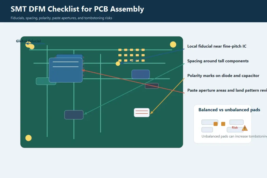
SMT DFM Checklist: Fiducials, Spacing, Paste, and Polarity
SMT assembly depends on stable paste printing, accurate placement, controlled reflow, and reliable inspection. The following SMT DFM checklist covers the design issues that most often affect yield.
Fiducials and Pick-and-Place Accuracy
Fiducials help the placement machine align the board or panel. They become more important on fine-pitch components, BGA/QFN packages, double-sided SMT, dense placement, and panelized production.
Check:
- Are global fiducials included?
- Are local fiducials needed near fine-pitch ICs, BGA, QFN, LGA, or dense areas?
- Are fiducials clear of solder mask, silkscreen, and nearby copper confusion?
- Are panel fiducials included if the board will be assembled in an array?
- Are tooling holes or rail features required by the assembly process?
- Are fiducials present in the same revision as the centroid data?
For many SMT lines, three well-placed global fiducials are preferred for board orientation and correction. Exact requirements should still be confirmed with the assembly supplier.
Component Spacing and Rework Access
Component spacing affects placement, soldering, AOI visibility, cleaning, coating, and rework.
Review:
- spacing between adjacent components
- spacing between tall components and small passives
- spacing around connectors, shields, transformers, inductors, and heat sinks
- edge clearance from routing paths, V-score, or mouse bites
- AOI and microscope visibility
- hand-soldering or rework access
- airflow and heat around power components
Dense layouts may be manufacturable, but density should be intentional. The practical question is not only whether the parts fit. The board also has to be placed, soldered, inspected, repaired, and tested without excessive risk.
Polarity, Pin 1, and Silkscreen Clarity
Unclear orientation is one of the simplest problems to prevent and one of the most frustrating to find during production.
Check orientation markings for:
- diodes
- LEDs
- electrolytic capacitors
- tantalum capacitors
- IC pin 1
- connectors
- switches
- relays
- modules
- batteries
Silkscreen, assembly drawing, centroid rotation, and BOM should agree. If there is not enough silkscreen space, make the assembly drawing clear enough for first article inspection and operator review.
Land Patterns and Solder Paste Openings
Land pattern and paste design influence solder volume, wetting, bridging, tombstoning, voiding, and reflow consistency.
Review:
- whether footprints match the selected MPNs
- whether the paste layer is present and correct
- whether paste apertures are suitable for fine-pitch parts
- whether exposed thermal pads need segmented openings
- whether small passives have balanced pad geometry
- whether copper connections create thermal imbalance
- whether via-in-pad or nearby vias may pull solder away
- whether alternate components share compatible footprints
For common packages, proven libraries and IPC-style land pattern thinking can reduce risk. For unusual packages, rely on the component datasheet and supplier review.
Tombstoning, Skew, and Solder Imbalance
Tombstoning occurs when a small passive lifts on one end during reflow. Skew happens when a part shifts from its intended position.
Risk increases when:
- pads are unbalanced
- one pad connects to a large copper area without thermal relief
- solder paste deposits are uneven
- components are very small, such as 0201 or 01005
- parts sit near high thermal mass areas
- reflow heating is uneven
Possible controls include pad balancing, thermal relief, aperture adjustment, component orientation review, and process tuning.
BGA, QFN, Fine-Pitch, and 0201/01005 Assembly Risks
BGA, QFN, LGA, CSP, fine-pitch ICs, and very small passives make compact electronic products possible. They also make assembly more sensitive to footprint quality, paste control, placement accuracy, inspection access, and rework planning.
PCBAgroup’s published assembly capability includes small passive component handling such as 01005, 0201, and 0402, fine-pitch parts, and BGA assembly with X-ray testing depending on board design. That capability helps, but the layout still has to support stable manufacturing.
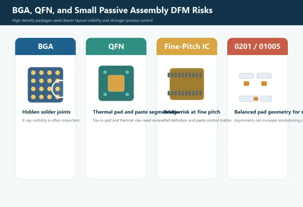
BGA and QFN Need Better Design Visibility
BGA and QFN solder joints are hidden or partly hidden. Visual inspection alone is not enough.
Review:
- pad size and solder mask definition
- package pitch
- via-in-pad requirements
- filled/capped via needs
- thermal pad design
- paste aperture percentage and segmentation
- X-ray inspection access
- rework clearance
- nearby heat-sensitive components
- board warpage risk
If a BGA or QFN fails inspection, rework may be possible, but it is slower and more controlled than ordinary SMT repair. Preventing the issue during design review is better than relying on rework later.
Fine-Pitch Components Increase Process Sensitivity
Fine-pitch components are more sensitive to solder mask registration, stencil aperture design, placement accuracy, and board cleanliness.
Check:
- pin pitch
- solder mask bridge feasibility
- paste aperture design
- pad length and width
- local fiducials
- AOI visibility
- solder bridge risk
- component spacing for rework
For very fine pitch, small deviations in footprint or paste design can create repeated defects.
0201 and 01005 Passive Components Require Stable Pad Design
Very small passives help miniaturize products, but they make pad symmetry and placement control more important.
Review:
- pad size and symmetry
- solder paste volume
- copper balance on both pads
- distance from large copper areas
- component orientation relative to reflow direction, if relevant
- inspection capability
- rework expectations
If the product does not truly need 01005 or 0201, a slightly larger passive package may improve yield, sourcing flexibility, and rework practicality. If the design does need them, treat them as a controlled process item rather than a casual footprint choice.
Through-Hole and Mixed Assembly DFM Rules
Through-hole assembly remains important for connectors, relays, transformers, switches, terminal blocks, high-current parts, and mechanically stressed components. Mixed SMT and THT designs are common in industrial control, power electronics, IoT gateways, equipment modules, and automotive-related products.
Hole Size, Lead Diameter, and Annular Ring
Through-hole soldering depends on correct mechanical and metallurgical fit.
Check:
- finished hole size
- lead diameter or pin size
- plating tolerance
- annular ring
- board thickness
- component seating height
- solder fill requirement
- lead protrusion after soldering
- compatibility with wave, selective, or manual soldering
If the finished hole is too tight, insertion becomes difficult. If it is too loose, solder fill and mechanical stability may suffer. Match the footprint to the exact component datasheet and supplier capability.
Connectors and Heavy Components Need Mechanical Planning
Connectors are both electrical and mechanical interfaces. Cable pull, repeated mating cycles, vibration, and enclosure fit can stress solder joints.
Review:
- connector orientation
- mounting pins or screws
- strain relief
- cable clearance
- enclosure interface
- support from mechanical housing
- staking or adhesive needs
- accessibility for soldering and inspection
For high-vibration products, through-hole connectors may offer stronger mechanical anchoring than SMT-only connectors. The right choice still depends on board space, current level, mating cycles, repair needs, and mechanical design.
SMT and THT Process Order Should Be Planned Early
Mixed technology boards may need reflow, wave soldering, selective soldering, hand soldering, cleaning, inspection, and testing in a specific order.
Check:
- Are bottom-side SMT parts compatible with wave exposure?
- Are tall components blocking selective solder nozzles?
- Are through-hole joints accessible?
- Are heat-sensitive parts too close to soldering areas?
- Are manual soldering steps minimized and controlled?
- Does cleaning need to happen after hand soldering or rework?
- Does coating happen after final test?
If the process route is unclear, quote and lead time may change after engineering review.
PCB Panelization for Assembly
Panelization is not only a PCB fabrication topic. It affects SMT handling, stencil printing, reflow transport, AOI, depanelization, labeling, and operator efficiency.
Why Panelization Matters for SMT Efficiency
Panelization helps:
- stabilize small boards during assembly
- support conveyor handling
- improve stencil printing consistency
- reduce manual handling
- create room for fiducials and tooling holes
- support traceability labels
- control depanelization
PCBAgroup’s assembly page states that boards smaller than 10 mm x 10 mm need panelization and that odd-shaped boards should be panelized with break-away rails at the two longer parallel edges for machine assembly. This is a practical example of why DFM should be reviewed before quotation.
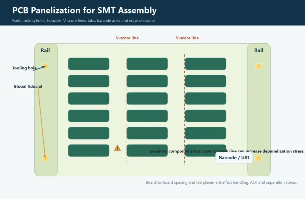
Rails, Tooling Holes, V-Cut, and Mouse Bites
Review:
- rail width and direction
- tooling hole position
- panel fiducials
- board-to-board spacing
- V-score direction
- mouse bite tab placement
- component clearance from rails and tabs
- orientation for SMT flow
- barcode or UID label position
Do not assume the PCB fabrication panel is automatically the best assembly panel. Fabrication yield and assembly handling sometimes require different priorities.
Depanelization Risk
Poor depanelization design can crack MLCCs, stress solder joints, damage board edges, or create cosmetic defects.
Review:
- whether sensitive parts are too close to tabs or V-score lines
- whether copper or traces are too close to routed edges
- whether the board shape creates stress concentration
- whether router depanelization is safer than manual breaking
- whether the panel leaves enough support for heavy components
For reliability-focused products, depanelization stress should be reviewed before the panel is released.
DFT Checklist: Test Points, Programming Ports, and Fixture Access
DFT turns manufacturing quality control into repeatable verification. Without test access, the factory may still build the board, but debug becomes slower and escape risk can increase.
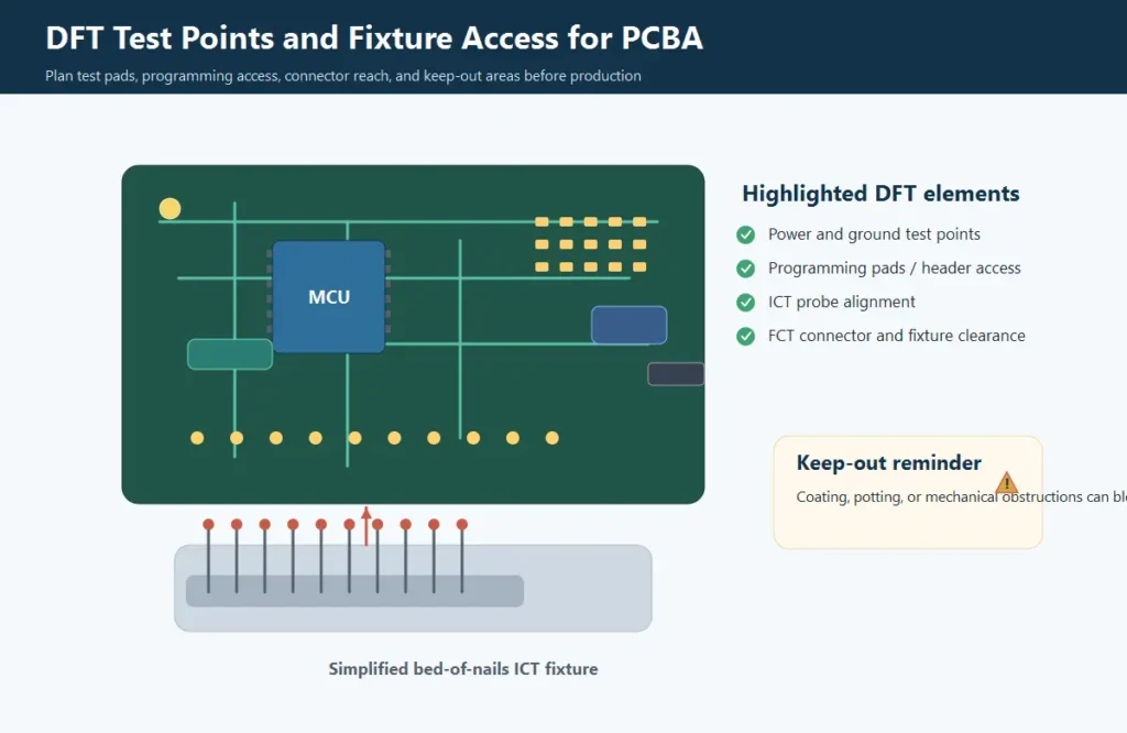
Test Points for ICT or Flying Probe
Test points allow electrical test equipment to contact important nets.
Review:
- ground and power test points
- key signal nets
- reset, boot, enable, and communication lines
- top or bottom access
- test pad size
- spacing between pads
- solder mask clearance
- distance from tall components
- fixture keep-out area
- whether coating or potting will cover test pads
Many fixtures prefer test pads around 0.8 mm or larger, but the real requirement depends on probe type, fixture design, test side, board density, and supplier capability. Confirm this with your PCBA manufacturer or test fixture provider.
Programming and Functional Test Access
If the board has an MCU, FPGA, wireless module, memory, calibration data, or bootloader, programming access should be designed early.
Clarify:
- programming interface, such as SWD, JTAG, UART, USB, SPI, or I2C
- connector or pogo-pad access
- power input during programming
- firmware file format
- firmware revision control
- verification method
- locking or security step
- serial number or calibration writing
FCT access should also be defined. If a product needs sensors, motors, displays, LEDs, buttons, communication ports, relays, loads, or calibration, the test fixture may require mechanical and electrical planning.
Test Requirements Should Match Product Risk
Do not over-test simple boards or under-test high-risk boards.
| Product Type | Typical Test Strategy Consideration |
|---|---|
| Simple prototype | Visual inspection, AOI, basic electrical or functional check may be enough |
| Dense SMT board | AOI plus X-ray for hidden joints where required |
| Industrial controller | Stronger electrical and functional verification is often justified |
| Firmware-driven board | Programming verification and FCT are usually important |
| High-reliability board | Test coverage, traceability, and environmental validation may be part of the plan |
The exact test strategy should match product risk, customer requirement, quantity, and cost of field failure.
Special Process Planning: Cleaning, Conformal Coating, Potting, and Labeling
Special processes are often forgotten in the first RFQ. When they appear later, they can change cost, lead time, component compatibility, and test sequence.
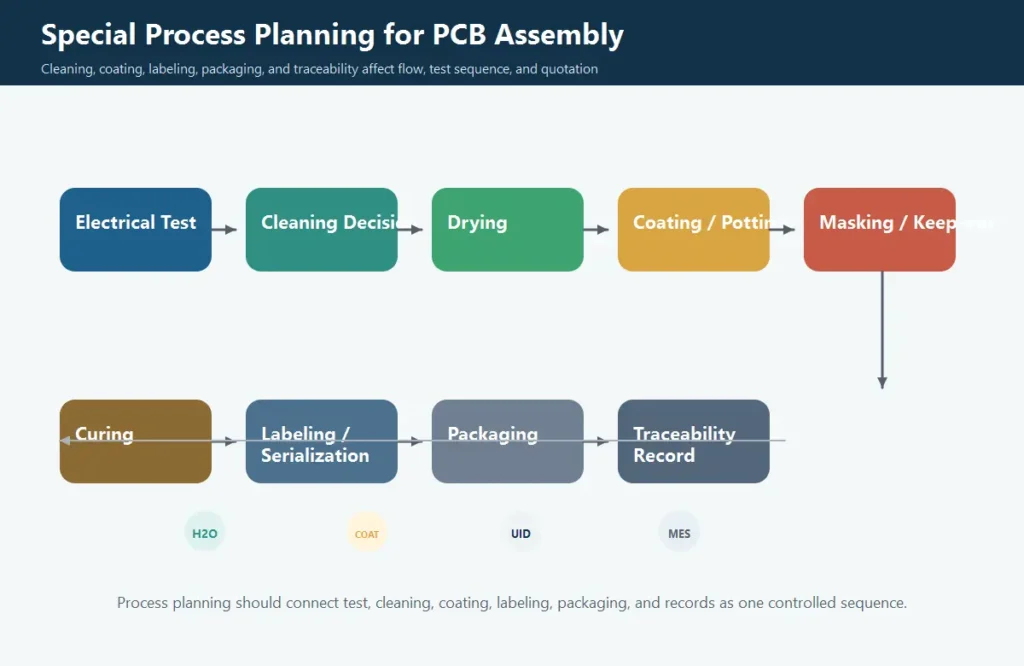
Cleaning and Ionic Contamination Requirements
Cleaning is not just cosmetic. Flux residue, ionic contamination, and handling contamination may matter for humid environments, high-impedance circuits, fine-pitch packages, coated boards, and long-life products.
Clarify:
- flux type preference
- whether no-clean residue is acceptable
- whether cleaning is required
- whether ionic cleanliness or ROSE testing is required
- whether components are sensitive to aqueous or ultrasonic cleaning
- drying requirement
- packaging after cleaning
Avoid absolute rules such as “all no-clean flux must be cleaned.” The right decision depends on product risk, environment, flux chemistry, board design, component compatibility, and customer requirements.
Conformal Coating Keep-Out Areas
Conformal coating can help protect PCBA products from moisture, dust, corrosion, and environmental contamination. It must be controlled rather than treated as a final cosmetic step.
Provide:
- coating area drawing
- keep-out area drawing
- material preference, if known
- thickness or inspection requirement, if specified
- masking requirement
- UV inspection requirement, if required
- curing requirement
- test sequence before and after coating
Common keep-out areas include:
- connectors
- sockets
- switches
- sensors
- test pads
- programming ports
- gold fingers
- heat sinks
- mounting holes
- grounding contacts
- LEDs or optical areas where coating affects function
Coating should not be used to hide poor cleaning, weak soldering, insufficient spacing, or inadequate enclosure design.
Potting, Staking, Adhesive, and Mechanical Reinforcement
Potting and staking can improve environmental or mechanical robustness, but they affect repairability, heat dissipation, weight, cost, and process flow.
Clarify:
- material type
- application area
- volume or thickness
- cure condition
- component compatibility
- thermal impact
- rework expectation
- inspection criteria
For heavy components, connectors, transformers, inductors, and vibration-sensitive products, mechanical reinforcement should be reviewed together with the enclosure and cable design.
Labels, Traceability, and Packaging
Production requirements are not limited to solder joints.
Define:
- label position
- barcode or QR code format
- serial number rule
- UID requirement, if any
- batch record requirement
- component lot traceability
- ESD packaging
- moisture-sensitive packaging
- tray, vacuum bag, or individual packaging
- carton label requirement
- shipment documentation
PCBAgroup’s quality page describes MES traceability that links process history, materials, operators, machines, parameters, and inspection records. If your project needs traceability or customer audit records, include that requirement in the RFQ.
Common DFM Mistakes That Increase PCBA Cost
Many PCBA cost problems do not come from material price alone. They come from repeated communication, rework, manual handling, weak test coverage, and late process changes.
Incomplete or Conflicting Files
This is one of the most common causes of quotation delay.
Examples:
- Gerber shows one footprint, BOM lists another package.
- Centroid rotation does not match assembly drawing.
- A connector orientation is unclear.
- Firmware revision does not match the test procedure.
- The latest BOM has DNP changes not reflected in placement data.
Solution: release one controlled file package for each build revision. File names should include project name, revision, and date.
Non-Standard Parts or Hard-to-Source Components
Uncommon packages, long-lead parts, EOL components, or single-source ICs can delay a project even when the PCB layout is sound.
Good BOM practice includes:
- exact MPNs
- approved alternates where allowed
- lifecycle and lead time review for critical parts
- customer approval process for substitutions
- clear consigned vs turnkey responsibility
This is where engineering and procurement need to work together. A layout is not truly production-ready if the key components cannot be sourced reliably.
Designs That Are Difficult to Inspect or Rework
High-density layouts are sometimes necessary, but they should not block inspection or rework unless that tradeoff is deliberate.
Risk examples:
- BGA too close to tall components
- QFN surrounded by heat-sensitive parts
- through-hole connector buried among dense SMT components
- test points hidden after enclosure assembly
- coating applied before final test access is used
- large MLCCs placed near depanelization tabs
Solution: review inspection and rework access as part of DFA, not after the first build fails.
PCBA DFM Checklist Before You Send the RFQ
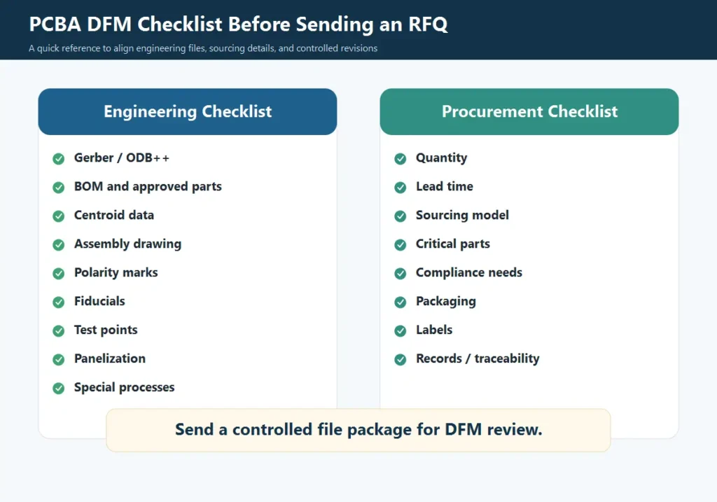
Engineering Checklist
- Gerber or ODB++ files are complete.
- Drill files and board outline are included.
- BOM, centroid, Gerber, and assembly drawing use the same revision.
- All MPNs and packages are confirmed.
- DNP/DNI parts are clearly marked.
- Approved alternates are listed where allowed.
- All polarity and pin 1 marks are clear.
- Fiducials are included at board or panel level.
- Fine-pitch, BGA, QFN, LGA, 0201, or 01005 parts are reviewed.
- Paste layer and thermal pad openings are checked.
- Via-in-pad requirements are controlled.
- SMT spacing supports placement, AOI, and rework.
- Through-hole holes match lead diameter and tolerance.
- Connectors and heavy components have mechanical support where needed.
- Panelization supports SMT handling and depanelization.
- Test points are planned for ICT, flying probe, programming, or FCT.
- Programming ports are accessible.
- Coating, cleaning, potting, staking, or labeling needs are marked.
- Product environment and reliability requirements are documented.
Procurement Checklist
- Quantity and quote breaks are clear.
- Prototype, pilot run, or production stage is stated.
- Target lead time is stated.
- Sourcing model is clear: turnkey, consigned, or partial turnkey.
- Critical components and long-lead parts are identified.
- Approved alternates are controlled by the customer.
- RoHS or other compliance requirements are stated where applicable.
- Packaging, labeling, and shipment needs are included.
- Inspection and test records required by the customer are defined.
- Payment, delivery, and logistics requirements are separated from technical assumptions.
RFQ Wording Example
Subject: RFQ for PCB Fabrication + PCB Assembly + DFM Review – [Project Name] Rev [X]
Attachments:
– Gerber or ODB++ files
– NC drill files
– BOM with MPNs and approved alternates
– Centroid / Pick-and-Place file
– Assembly drawing
– Test requirements
– Special process notes, if applicable
Project stage:
Prototype / pilot run / mass production
Expected quantity:
[Quantity and quote breaks]
Sourcing model:
Turnkey / consigned / partial turnkey
Product application:
[Example: industrial IoT controller used in high-humidity equipment cabinet]
Assembly notes:
SMT + THT mixed assembly. BGA and QFN packages included. Please review DFM, DFA, DFT, panelization, and test access before quotation.
Testing requirements:
AOI, X-ray for hidden joints where required, programming, and FCT according to attached test procedure.
Special requirements:
Cleaning / conformal coating / potting / labeling / traceability, if required.
Requested feedback:
Please provide quotation, lead time, key DFM risks, sourcing risks, and any file questions before production.
How PCBAgroup Reviews DFM Risks Before Production
PCBAgroup’s published service pages describe PCB assembly support across SMT, through-hole, and mixed assembly, with turnkey, consigned, and partial turnkey sourcing options. The site also lists small passive component assembly capability, BGA and fine-pitch handling, laser-cut stainless steel stencils, X-ray testing for BGA, and panelization needs for small or odd-shaped boards.
For a PCBA DFM review, PCBAgroup can evaluate project risks before production based on the file package and application requirements.
File Review and Engineering Feedback
The review may include:
- Gerber or ODB++ completeness
- drill and board outline review
- panelization and rail needs
- BOM and footprint consistency
- centroid and assembly drawing alignment
- polarity and pin 1 review
- SMT spacing and placement review
- BGA, QFN, fine-pitch, and small passive risk review
- through-hole and mixed assembly process review
- test access and fixture planning
- cleaning, coating, potting, labeling, and packaging notes
- revision control before production release
SMT, THT, Inspection, and Testing Support
PCBAgroup’s website lists process and quality-control steps including process review, IQC, SPI solder paste inspection, online AOI, first sample test, offline AOI, X-ray inspection for hidden solder joints, and manual QC inspection.
Its quality page also describes MES traceability, real-time quality data, standardized work instructions, and an environmental and performance testing lab with temperature and humidity, simulated transportation vibration, salt spray, battery testing, and BGA rework support.
Those capabilities matter because DFM should connect directly to production control, inspection, testing, and traceability. A useful review does not stop at “can we place the parts?” It asks whether the board can be built, checked, tested, recorded, and repeated.
From Prototype Validation to Mass Production
The best time for DFM review is before production, not after defects appear.
For prototype builds, the goal is to identify footprint, placement, assembly, sourcing, and test risks early. For pilot runs, the focus shifts to process settings, test coverage, rework needs, and packaging. For mass production, repeatability, traceability, and change control become more important.
If you are preparing a PCBA project, send your Gerber or ODB++ files, BOM, centroid file, assembly drawing, test requirements, quantity, sourcing model, and application environment to PCBAgroup for engineering review and quotation.
FAQ
What is DFM in PCB assembly?
DFM in PCB assembly means reviewing a PCB design and production file package before manufacturing to confirm that the board can be fabricated, assembled, inspected, tested, and scaled with acceptable cost, yield, and reliability. It includes PCB fabrication data, component footprints, SMT and THT process risks, panelization, test access, special processes, and revision control.
What is the difference between DFM, DFA, and DFT?
DFM focuses on manufacturing feasibility, DFA focuses on assembly efficiency, and DFT focuses on production testability. In PCBA projects, all three are connected. A board that is easy to fabricate may still be difficult to assemble or test if component spacing, polarity, fixture access, or test points are not planned correctly.
When should I request a DFM review?
Request DFM review before the layout is frozen whenever possible. At minimum, request it before prototype production. For high-density designs, BGA/QFN packages, 0201/01005 components, mixed SMT/THT assembly, high-reliability products, or tight delivery schedules, early DFM review should be treated as a required project step.
What files are needed for a PCBA DFM review?
Prepare Gerber or ODB++ files, NC drill files, BOM with MPNs, centroid file, assembly drawing, quantity, sourcing model, and test requirements. For complex builds, also provide schematic, fabrication drawing, STEP file, programming instructions, coating or cleaning requirements, product environment, and reliability expectations.
Does DFM reduce PCB assembly cost?
Yes. DFM can reduce cost by improving SMT yield, reducing manual rework, simplifying panelization, improving test access, avoiding fixture redesign, and reducing engineering clarification time. The biggest savings often come from preventing problems before production rather than repairing boards after defects appear.
How much component spacing is required for SMT assembly?
There is no universal spacing rule that fits every board. Spacing depends on component package, placement equipment, soldering process, AOI visibility, rework access, coating or cleaning needs, and supplier capability. Ask your PCBA manufacturer to review actual spacing against your component list and production process.
Why does my supplier ask for test points?
Test points allow ICT, flying probe, programming, and fixture-based tests to contact important nets reliably. Without test access, production testing may become slower, less complete, or more dependent on manual troubleshooting. Test points are especially important for repeat production and high-reliability products.