Table of Contents
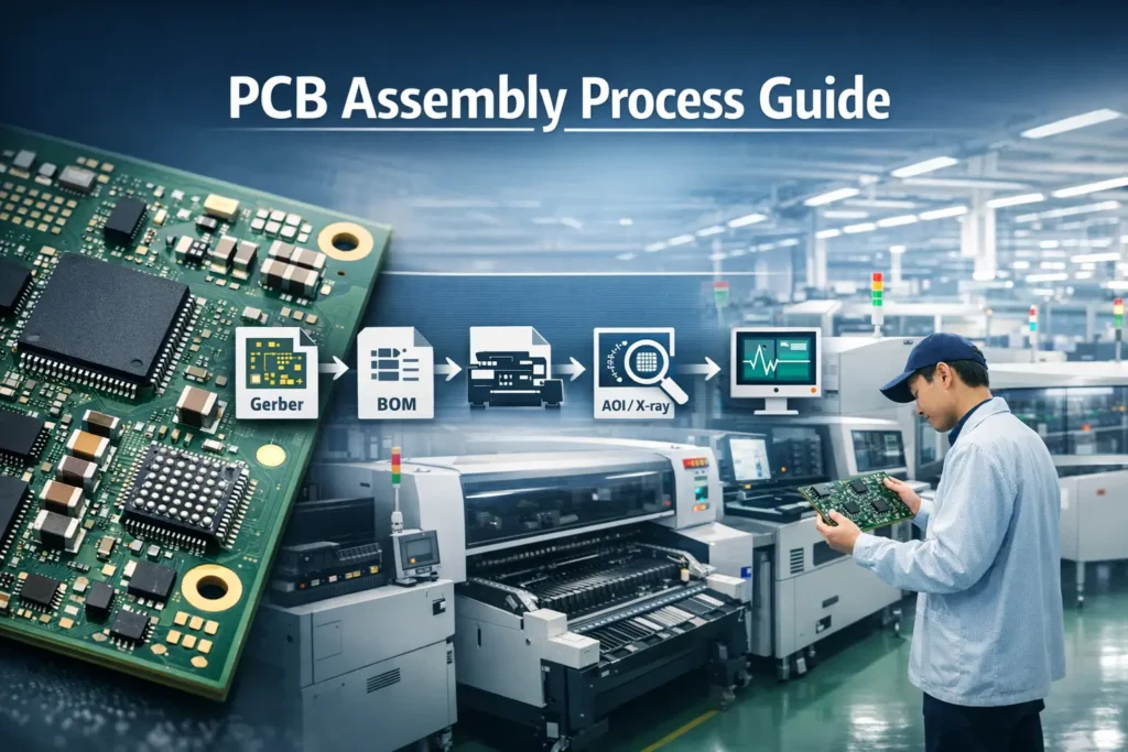
PCB Assembly Process: A Practical Guide from Prototype to Production
For engineers, OEMs, and electronics buyers, understanding the PCB assembly process is essential to building reliable products, controlling lead time, and reducing manufacturing risk. Whether you are developing an industrial controller, medical device, communication product, power module, or consumer electronics hardware, the way a PCB is assembled has a direct impact on performance, consistency, and long-term reliability.
This guide explains the full PCB assembly process step by step, from engineering review and file preparation to SMT, through-hole assembly, inspection, testing, and shipment. It also covers how SMT, THT, and mixed assembly differ, how prototype builds are managed compared with low-volume and mass production, and what to look for when choosing a PCB assembly manufacturer.
If you are evaluating a new project or comparing suppliers, this article is designed to help you understand both the technical process and the practical decisions behind successful PCBA manufacturing.
What Is PCB Assembly?
PCB assembly, or Printed Circuit Board Assembly, is the process of mounting and soldering electronic components onto a bare printed circuit board so that it becomes a functional electronic unit.
A bare PCB only provides the physical structure and conductive pathways. It does not perform any electronic function on its own. Once resistors, capacitors, ICs, connectors, power devices, and other components are accurately placed and soldered onto the board, it becomes a PCBA that can process signals, control power, communicate with other systems, or perform its intended electronic function.
In simple terms, PCB assembly is the process that gives a circuit board its working life. It transforms a passive substrate into the functional core of an electronic product.
Modern PCB assembly generally includes three main approaches:
SMT (Surface Mount Technology) for compact, automated, high-density assembly
THT (Through-Hole Technology) for mechanically strong or high-power components
Mixed assembly, which combines SMT and THT on the same board when the design requires both miniaturization and mechanical robustness
A complete PCB assembly process typically includes solder paste printing, component placement, reflow soldering, through-hole insertion, inspection, electrical testing, and final packaging.
PCB vs PCBA: What’s the Difference?
A PCB is the bare printed circuit board. It consists of the substrate, copper traces, solder mask, silkscreen, and drilled or plated holes, but no electronic components are installed.
A PCBA is the finished assembled board. It includes the bare PCB plus all mounted and soldered components, and it is normally inspected and tested before delivery.
This distinction matters because PCB fabrication and PCB assembly are different manufacturing stages with different files, equipment, lead times, and control points. PCB fabrication focuses on producing the board itself. PCB assembly focuses on turning that board into a working electronic module.
Where PCB Assembly Fits in Electronics Manufacturing
PCB assembly sits at the critical stage between circuit design and final product manufacturing.
It is the process that turns electrical design data into a real, testable, functional hardware platform. Without assembly, the design remains only a layout file. With assembly, it becomes a working board that can be validated, integrated, and delivered.
PCB assembly also has a direct effect on:
product electrical performance
solder joint reliability
field durability
manufacturability
production yield
time to market
In high-reliability applications such as industrial electronics, medical equipment, automotive-adjacent control systems, and aerospace support hardware, assembly quality is not just a manufacturing issue. It is a core product quality issue.
What Files Are Needed Before PCB Assembly Starts?
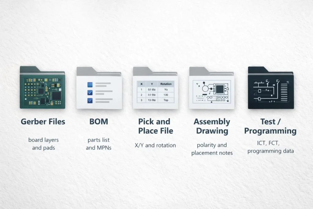
Before PCB assembly begins, the manufacturer needs a complete and accurate documentation package. This is one of the most important stages in the whole process, because incomplete or inconsistent files can cause quotation errors, NPI delays, sourcing problems, programming mistakes, and avoidable engineering questions.
Clear documentation reduces NPI delays and quotation errors.
A professional PCB assembly manufacturer will typically request the following files.
Gerber Files
Gerber files are the digital blueprint of the PCB layout. They define the copper layers, drill holes, solder mask openings, silkscreen, pad geometry, and board outline.
For assembly, Gerber data is used not only to understand the board structure, but also to prepare SMT stencils and support DFA or DFM review. Engineers use the files to confirm whether pad geometry, solder mask clearances, and board layout are suitable for assembly.
For most projects, the most relevant layers include:
copper and pad layers
solder mask layers
silkscreen layers
drill files
board outline
If customers do not want to share a full design package for confidentiality reasons, NDA protection and controlled file sharing are commonly used.
Bill of Materials (BOM)
The BOM is the core document for purchasing, kitting, and assembly planning. It lists every component required to build the board.
A complete BOM should include:
reference designator
manufacturer name
manufacturer part number
description
package type
quantity
mounting type
approved alternates if available
For turnkey PCB assembly, BOM quality directly affects sourcing speed, cost accuracy, and build readiness. During engineering review, the BOM is checked against the PCB design to identify issues such as obsolete parts, package mismatches, inconsistent descriptions, or missing data.
Pick and Place / Centroid File
This file provides the X/Y coordinates, board side, and rotation angle for each SMT component. It is used to generate the placement program for pick-and-place machines.
If the file is missing, engineers may need to extract or measure placement data manually from the Gerber files, which increases both engineering time and the risk of setup errors. For efficient SMT programming, a correct centroid file is highly recommended.
Assembly Drawings and Special Instructions
Assembly drawings show component placement, orientation, polarity, and any special build requirements. These drawings are especially useful for first article inspection, manual insertion steps, and verification of polarized or non-standard parts.
Special instructions may include:
jumper wires
glue or staking points
panelization requirements
selective soldering zones
conformal coating areas
cleaning requirements
specific assembly sequence
special marking or labeling instructions
For complex assemblies, these files help prevent misunderstandings that BOM and coordinate data alone cannot resolve.
Test Requirements and Programming Files
If the assembled board requires ICT, flying probe, firmware loading, programming, or functional testing, these instructions should be defined before production.
This may include:
test procedures
pass/fail criteria
test fixture requirements
programming files
firmware or bootloader data
calibration steps
communication interface checks
Although not always mandatory, schematics and fabrication drawings are also helpful when engineering teams need to troubleshoot, design test fixtures, or confirm material and process compatibility.
PCB Assembly Process Step by Step
The PCB assembly process follows a structured production workflow. The exact sequence can vary by project type, board complexity, and manufacturing model, but most assemblies go through the following stages.
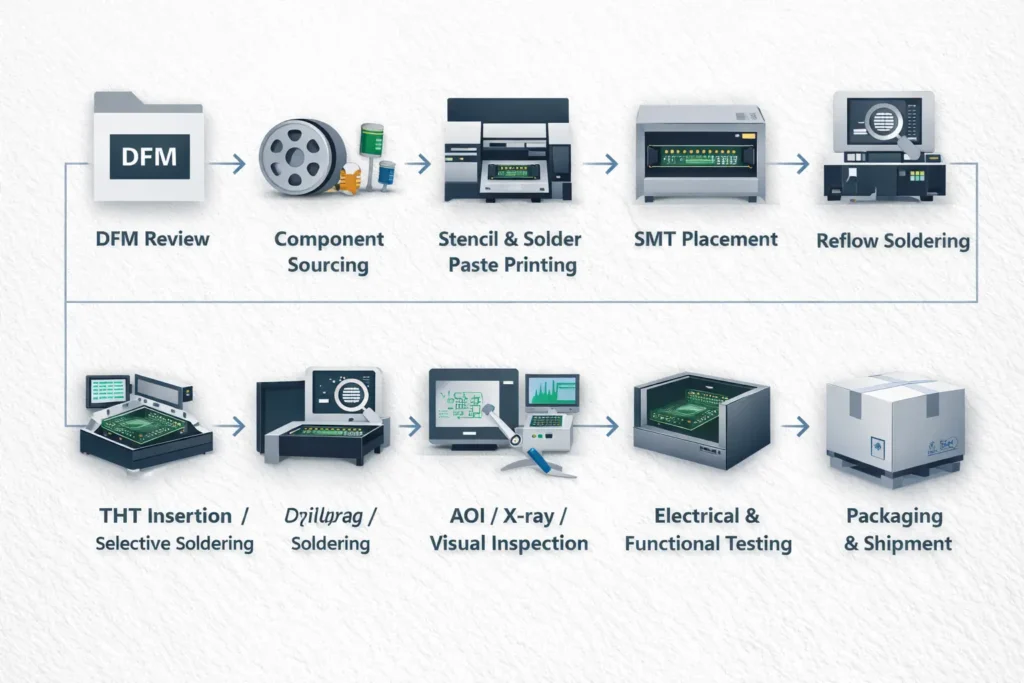
1. DFM and Engineering Review
Design for Manufacturability review is the first critical checkpoint before production.
Its purpose is to verify that the board can be assembled efficiently, consistently, and within the actual capability of the factory’s process and equipment. A good DFM review does more than check design rules. It evaluates whether the design is practical for real-world manufacturing.
Typical review points include:
package and footprint consistency
component spacing
polarity clarity
pad design suitability
solder mask opening adequacy
fiducial placement
panelization method
assembly side planning
test point accessibility
connector clearance
heat-sensitive component placement
special process needs such as BGA, QFN, coating, or selective soldering
This stage often involves cross-functional coordination between design engineering, manufacturing engineering, and quality teams. It is one of the most effective ways to prevent yield problems, rework, and production delays later.
2. Material Preparation and Component Sourcing
Once the file package is approved, the project moves into material preparation.
For turnkey PCB assembly, the contract manufacturer sources all required components and bare boards. For consigned or partial-turnkey models, the supplier coordinates incoming materials from both customer and distributor channels.
At this stage, the key concerns are:
authentic components from reliable supply channels
lead time and availability
substitute approval rules
moisture-sensitive device handling
PCB flatness and solderability
lot consistency and storage conditions
Moisture-sensitive devices may need controlled storage and baking before use. PCB bare boards are also checked for surface finish quality, pad condition, solder mask integrity, and mechanical specification compliance.
3. Stencil Making and Solder Paste Printing
For SMT assemblies, solder paste printing is the beginning of the actual line process.
A stencil is fabricated based on the PCB pad design. The thickness and aperture design of the stencil determine solder paste volume, which directly affects solder joint quality. Fine-pitch ICs, BGAs, and components with different pad geometries may require optimized aperture design or step stencils.
During printing, the stencil is aligned with the PCB and solder paste is deposited onto the pads using a controlled squeegee process. Print pressure, speed, separation distance, and paste condition must all be controlled to ensure stable results.
Many production lines use SPI (Solder Paste Inspection) immediately after this step to measure paste height, area, volume, and offset. This helps detect printing defects before components are placed.
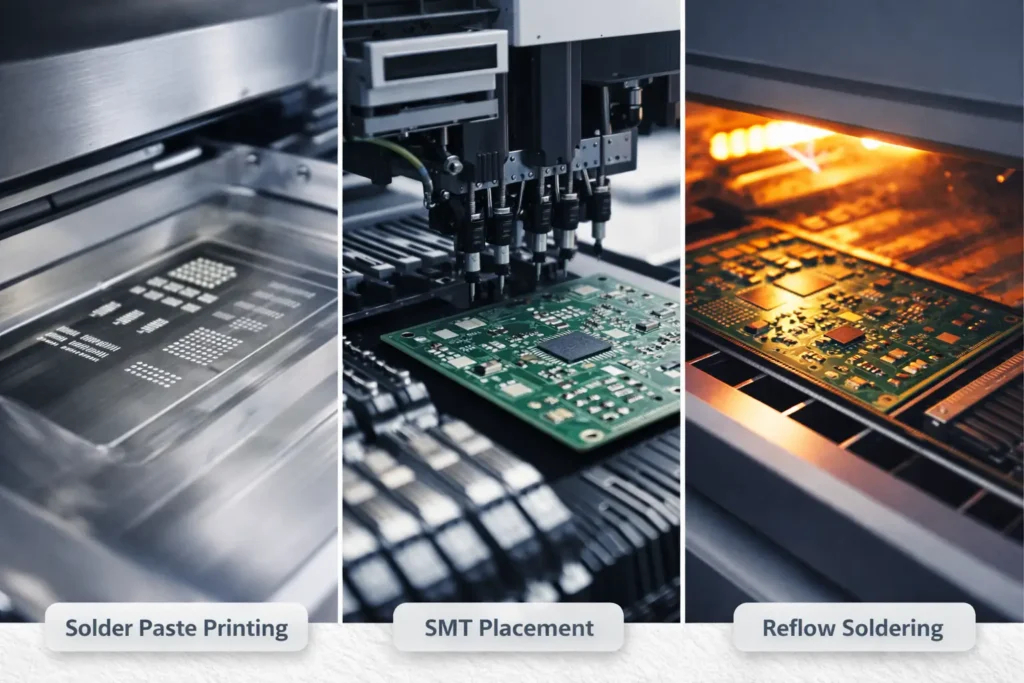
4. SMT Component Placement
After solder paste printing, SMT components are mounted by pick-and-place machines.
The placement machine uses the centroid file and vision alignment systems to identify fiducials and position components accurately on the board. Modern placement systems can handle everything from very small chip components to fine-pitch ICs, QFNs, and BGAs with high accuracy and high speed.
Placement performance depends on:
machine accuracy
feeder setup quality
component packaging consistency
vision recognition reliability
correct nozzle selection
stable program data
For high-density assemblies, especially with BGA or bottom-terminated devices, this stage requires precise process control.
5. Reflow Soldering
Once all SMT components are placed, the boards move through a reflow oven.
The reflow process melts the solder paste and permanently bonds the components to the PCB pads. A typical reflow profile includes preheat, soak, reflow, and cooling stages. Each stage must be controlled according to the solder alloy, board thermal mass, and component heat tolerance.
If the thermal profile is poorly controlled, it can cause:
insufficient wetting
tombstoning
solder voiding
head-in-pillow defects
component shift
overheating damage
board warpage
For lead-free assembly, peak temperatures typically fall within a higher process window than traditional tin-lead soldering. In some high-reliability or advanced applications, nitrogen reflow may be used to reduce oxidation and improve solder quality.
6. THT Insertion and Wave/Selective Soldering
Boards that include through-hole components go through a separate insertion and soldering stage after SMT, or in a combined mixed-assembly workflow.
Through-hole parts may include:
connectors
transformers
relays
electrolytic capacitors
high-power devices
mechanically stressed terminals
Insertion may be manual or semi-automated depending on component type and volume. Soldering is then completed by one of the following methods:
manual soldering
wave soldering
selective soldering
For mixed-technology boards, selective soldering is often preferred because it applies heat only to specific locations and reduces thermal stress on already assembled SMT components.
7. AOI, X-ray, and Visual Inspection
After soldering, the boards go through inspection to identify defects before electrical testing.
AOI
Automated Optical Inspection is widely used both before and after reflow.
Pre-reflow AOI can detect:
missing parts
wrong parts
polarity reversal
placement offset
Post-reflow AOI can detect:
insufficient solder
excess solder
bridging
lifted leads
tombstoning
component shift
X-ray Inspection
X-ray inspection is essential for packages with hidden solder joints, such as BGAs, CSPs, and QFNs with thermal pads.
It helps identify:
voids
hidden bridges
missing balls
insufficient collapse
internal solder anomalies
In high-reliability applications, BGA inspection is especially important because visual inspection alone cannot confirm joint integrity.
Visual Inspection
Manual visual inspection remains useful as a support layer, especially for labels, workmanship, connector seating, and final appearance verification. It is commonly performed according to IPC workmanship standards.
8. Electrical Testing and Functional Testing
Inspection confirms physical build quality. Testing confirms electrical and functional performance.
Depending on the product and volume, different testing methods may be used.
Flying Probe Testing
Flying probe testing uses movable probes to check continuity, shorts, and component-level values without requiring a dedicated fixture. It is especially useful for prototypes, low-volume orders, and frequently revised designs.
ICT
In-circuit testing uses a custom fixture to contact all test points simultaneously. It is highly efficient for stable, medium- to high-volume production and can quickly identify assembly defects such as opens, shorts, and wrong-value components.
Functional Testing
Functional testing powers up the board and simulates its real operating condition. It verifies whether the PCBA performs as intended under defined test criteria.
This is often the final and most important production-level validation step for product function. Depending on the application, it may also include firmware programming, communication checks, calibration, burn-in, or environmental verification.
9. Conformal Coating, Cleaning, Box Build, or Final Assembly
Some products require additional post-assembly processes after testing.
These may include:
board cleaning
conformal coating
potting or staking
depaneling
cable harness installation
enclosure integration
label application
serial number marking
final box build
Conformal coating is especially common for electronics exposed to humidity, dust, salt spray, or harsh industrial environments. Cleaning may also be required when flux residue could affect reliability.
10. Packaging and Shipment
The final stage is packaging and shipment.
PCBAs are packed according to their fragility, ESD sensitivity, product geometry, and shipping route. Common packaging solutions include anti-static bags, blister trays, ESD foam, vacuum packaging, and shock-resistant outer cartons.
For export shipments, proper packaging is part of quality control. A well-built board can still fail in transit if packaging does not adequately protect against electrostatic discharge, vibration, or impact.
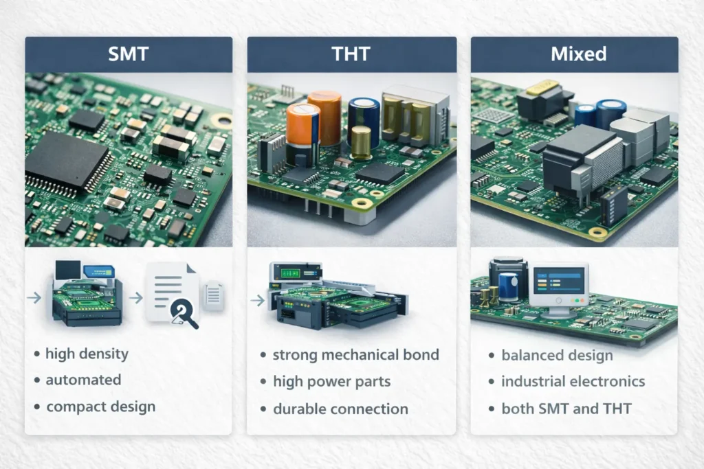
SMT vs THT vs Mixed Assembly: Which One Is Right for You
Choosing the right assembly method depends on board function, mechanical stress, product size, current requirements, signal performance, and production volume.
When SMT Is the Better Choice
SMT is the dominant technology in modern electronics manufacturing and is usually the best choice when the design requires:
miniaturization
high component density
double-sided assembly
automated production
high-speed digital or RF performance
advanced package support such as BGA, QFN, CSP, or fine-pitch ICs
Because SMT components are smaller and have shorter interconnect paths, they support better signal integrity and more efficient use of PCB space. SMT also offers very high throughput in automated manufacturing, making it the preferred solution for most commercial electronics.
When THT Is Still Necessary
THT remains important when components must withstand higher mechanical load, repeated insertion forces, or higher thermal stress.
Typical THT use cases include:
power connectors
relays
transformers
large electrolytic capacitors
high-power transistors
industrial terminals
mechanically stressed electromechanical components
THT is also useful for prototypes, repair work, and specialized high-reliability assemblies where manual access and strong physical anchoring are important.
When Mixed Assembly Makes Sense
Mixed assembly is common in real-world industrial products because many boards require both compact signal processing and physically robust power or interface components.
It is often used in:
industrial control systems
power electronics
networking equipment
automotive control modules
medical electronics
server and communication hardware
A mixed approach allows designers to use SMT for dense control circuitry and THT for connectors, transformers, and mechanically stressed parts, optimizing both performance and reliability.
Manual vs Automated PCB Assembly
The balance between manual and automated assembly depends on product stage, board complexity, and production volume.
Best Use Cases for Manual Assembly
Manual assembly is most suitable for:
prototypes
engineering samples
very low-volume production
unusual or oversized components
special THT operations
rework and repair
custom builds with frequent design changes
It offers flexibility and fast adaptation, especially when the design is still being validated.
When Automation Improves Cost and Consistency
Automation becomes increasingly valuable when the project requires:
repeatable quality
high placement accuracy
volume efficiency
lower long-term manufacturing cost
better traceability
stable production scheduling
Automated placement and controlled soldering processes reduce dependence on manual skill variation, minimize human error, and improve yield consistency across larger production lots.
For companies expecting a project to scale, choosing a supplier with both prototype flexibility and automated production capability is usually the better long-term decision.
Prototype, Low-Volume, and Mass Production PCBA
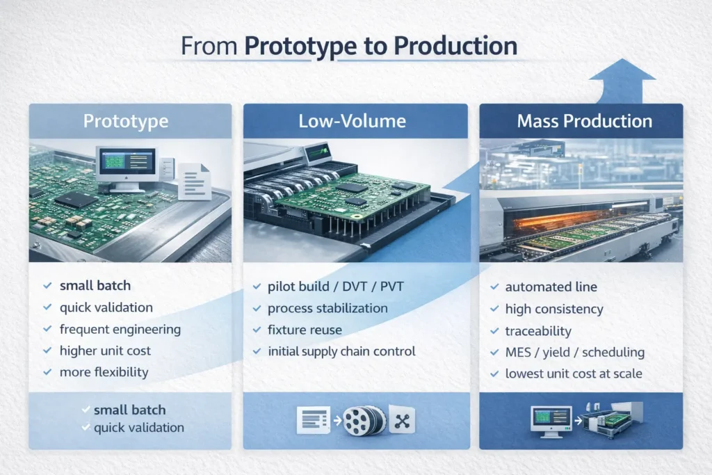
PCB assembly strategy should change as the product moves from engineering validation to commercial production. A prototype build is not managed the same way as a recurring production order.
Prototype PCB Assembly
Prototype assembly is focused on speed, flexibility, engineering verification, and fast feedback.
At this stage, the priorities are:
rapid turnaround
DFM feedback
design validation
BOM verification
process feasibility
functional confirmation
Prototype orders are usually small, often one to ten boards, which means NRE costs such as stencil making, program setup, engineering review, and test preparation are spread over very few units. This makes unit cost higher, but the value lies in fast learning and fast iteration.
Material sourcing for prototypes also requires a different strategy. Since quantities are low, the focus is on availability, minimum packaging, and quick procurement rather than on bulk price optimization. Good prototype suppliers reduce waste by buying efficiently and using flexible production setups.
Quality control at this stage is not just about catching solder defects. It is also about discovering design risks and assembly challenges before the product moves forward.
Low-Volume Production
Low-volume production is often used for pilot runs, DVT or PVT phases, industrial equipment, market testing, and custom products.
At this stage, the process begins shifting from engineering flexibility toward process repeatability. The manufacturer needs to balance responsiveness with more structured planning.
Compared with prototypes, low-volume runs allow:
partial NRE cost distribution
more stable fixture reuse
more efficient panelization
tighter process parameter control
better purchasing planning
early traceability setup
This is often the stage where a supplier proves whether it can move a project toward stable production without losing speed or communication quality.
Medium-to-High Volume Production
When the product enters medium- or high-volume production, the focus shifts to scale, repeatability, supply chain stability, and cost optimization.
Priorities now include:
supply chain coordination
stable material planning
automated inspection
fixture-based testing
MES-driven traceability
process control by data
consistent delivery scheduling
At this stage, the cost structure changes significantly. Engineering setup costs are spread across many units, procurement becomes more strategic, and factory efficiency becomes a major factor in competitiveness. Process control also becomes more preventive and data-driven, with real-time monitoring of furnace profiles, defect trends, lot traceability, and inspection results.
For mature products, the right manufacturing partner should be able to support this scale without forcing a disruptive transfer to a new supplier.
How Quality Is Controlled in the PCB Assembly Process
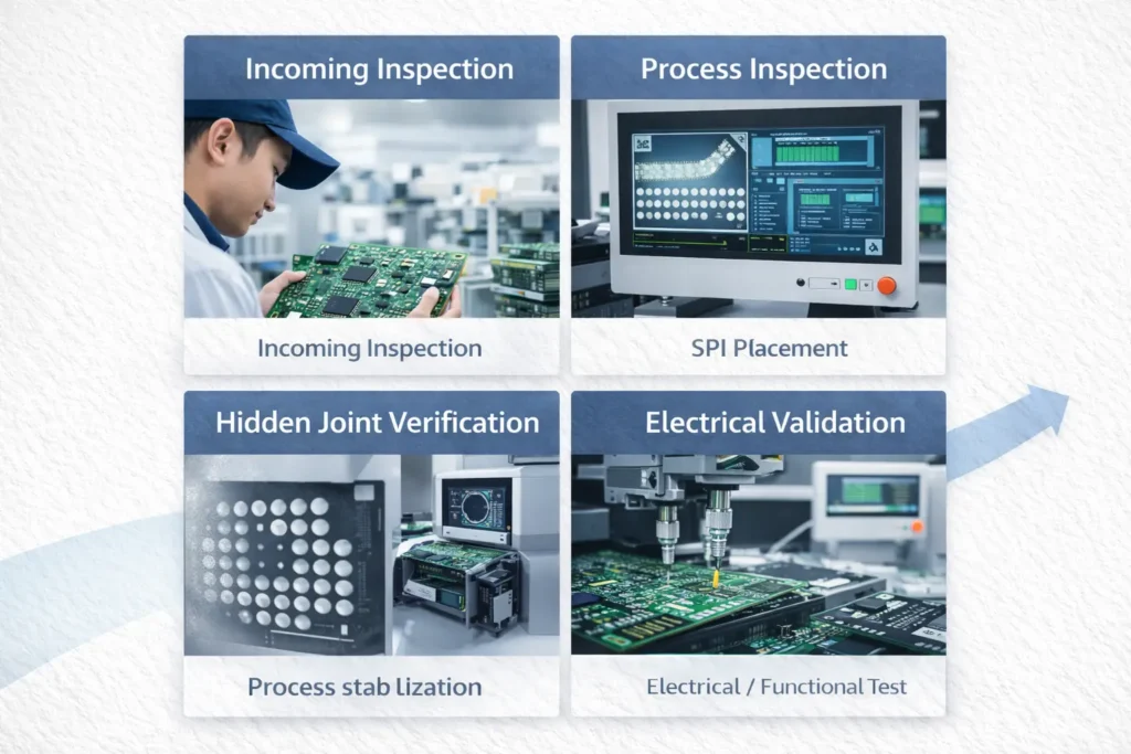
Quality control in PCB assembly should not rely on a single inspection step. It is built through layered control from incoming materials to final shipment.
Incoming Material Inspection
Incoming inspection verifies that the PCB bare boards and electronic components match the approved documentation and are suitable for production.
This may include:
packaging and label checks
date code and batch verification
part number confirmation
quantity checks
PCB appearance review
dimension and thickness verification
solderability checks
moisture control review
storage condition validation
For critical or high-reliability products, incoming inspection may also include internal structure confirmation or lot-level documentation review.
SPI / AOI / X-ray Inspection
These three methods form the core visual control system in modern SMT manufacturing.
SPI
SPI measures solder paste deposits in three dimensions after printing. It helps detect issues such as insufficient volume, offset, bridging, or poor stencil release before the board continues down the line.
AOI
AOI detects placement and soldering defects by comparing the assembled board against programmed standards. It is one of the most effective ways to identify missing parts, wrong parts, polarity errors, lifted leads, solder bridges, and visible workmanship defects.
X-ray
X-ray inspection is critical for hidden joints under BGA, CSP, QFN thermal pads, and similar packages. It is the main non-destructive tool for evaluating these joints internally.
For BGA-heavy products, X-ray should be treated as a normal process requirement rather than an optional extra.
First Article Inspection
First article inspection validates the first completed board or first batch before regular production continues.
Its purpose is to catch setup mistakes, wrong materials, incorrect polarity, programming issues, tooling errors, or process mismatches before they affect the full order.
For new product introduction, first article inspection is one of the most important gates in the production workflow.
Flying Probe, ICT, and Functional Test
Each testing method serves a different purpose.
Flying probe is flexible and cost-effective for prototypes and small batches
ICT is fast and powerful for stable, higher-volume builds
Functional test verifies whether the board works in real operating conditions
A strong testing strategy uses the right method for the right stage of the project, rather than applying the same test plan to every order.
Traceability and Process Control
In mature manufacturing, quality is not only about inspection. It is also about traceability and control.
Traceability allows each board or batch to be linked to:
component lot information
bare board batch
machine programs
oven profiles
operator records
inspection results
test data
shipment records
Process control means monitoring critical parameters in real time so that deviations can be corrected before they become defects. In larger-scale production, this often includes MES integration, SPC methods, alarm systems, and process history review.
For industrial, medical, and other reliability-focused products, traceability is a major advantage.
Common PCB Assembly Issues and How to Prevent Them
Many PCB assembly problems can be prevented if they are addressed before production begins.
Missing or Incorrect BOM Data
A poorly managed BOM can lead to quotation mistakes, part substitutions, purchasing delays, and wrong-part installation.
To prevent this:
use standardized BOM templates
apply version control
keep library data consistent
verify MPNs and footprints
confirm purchasing availability before release
align BOM updates with ECO or ECN changes
Insufficient Component Spacing
Spacing problems can create both assembly risk and electrical safety risk. Tight spacing may cause solder bridging, rework difficulty, or even insulation failure in high-voltage products.
The best prevention methods are:
follow the manufacturer’s DFM rules early
verify spacing by DRC and DFM tools
optimize layout for assembly access
review tall component and connector clearance
consider creepage and clearance where applicable
Poor Solderability or Moisture-Sensitive Parts
Oxidized pads, contaminated leads, or moisture-sensitive devices can cause weak joints, voiding, or component damage during reflow.
To reduce risk:
use controlled storage
manage MSD parts according to handling standards
bake components when required
maintain proper workshop humidity
follow correct solder paste storage and use rules
avoid direct hand contact with solderable surfaces
BGA Inspection Challenges
BGA packages are difficult because the solder joints are hidden under the component.
Good control requires:
X-ray inspection
clear acceptance criteria
proper reflow profiling
strong alignment control
electrical test support where possible
traceable inspection records
Late Design Changes Before Production
Late ECO changes can create major disruption if files, materials, and setup data are not synchronized.
To avoid confusion:
use strict revision control
update Gerber, BOM, centroid, and drawings together
clearly define the effective build revision
isolate old and new materials
confirm change cost and lead-time impact before release
How to Choose a Reliable PCB Assembly Manufacturer
For engineers and buyers, choosing a PCB assembly manufacturer is not only about comparing unit price. The better question is whether the supplier can reduce risk, support your project stage, and maintain quality as volume grows.
Engineering Support and DFM Feedback
A strong manufacturing partner should provide more than build-to-print execution. It should be able to review your files, identify risks early, and give practical manufacturability feedback based on real process capability.
Look for suppliers that can support:
DFM review before production
package and footprint checks
panelization suggestions
soldering process advice
test strategy planning
assembly risk identification
Component Sourcing Capability
For turnkey projects, sourcing capability is critical.
A reliable supplier should have:
access to trusted distributor and manufacturer channels
strong purchasing communication
alternate part management
shortage response procedures
controlled storage for sensitive materials
inventory discipline for recurring builds
This matters even more when global component availability is unstable.
Inspection and Testing Resources
Do not assume every assembly supplier has the same inspection depth.
Ask whether the supplier can support:
SPI
AOI
X-ray
flying probe
ICT
functional test
programming
conformal coating
reliability-related verification if needed
A supplier’s equipment list alone is not enough. It should also have a disciplined process for using those tools effectively.
Prototype-to-Production Scalability
Many projects start small and scale later. A valuable supplier is one that can support prototypes, pilot builds, and recurring production in one operational system.
This helps reduce:
communication loss
transfer risk
repeated setup work
process inconsistency between vendors
Communication, Lead Time, and Supply Chain Location
In overseas manufacturing, communication quality matters just as much as process capability.
A strong supplier should provide:
fast response to engineering questions
transparent status updates
realistic lead times
stable export handling
practical logistics support
dependable schedule control
A capable factory in the right supply chain location can make a major difference to both delivery speed and project stability.
Why Shenzhen Is Strong for PCB Manufacturing and Assembly
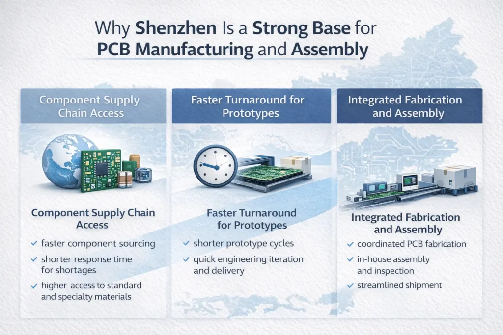
For global OEMs and electronics buyers, Shenzhen remains one of the most efficient locations for PCB manufacturing and assembly.
Component Supply Chain Access
Shenzhen benefits from one of the world’s most concentrated electronics supply ecosystems.
This brings several practical advantages:
faster component sourcing
shorter response time for shortages
easier access to standard and specialty materials
better coordination between procurement and production
reduced logistics friction across the supply chain
For customers, this often translates into faster quoting, shorter NPI cycles, and more responsive material support.
Faster Turnaround for Prototypes
Speed matters in electronics development. Shenzhen’s manufacturing ecosystem is especially strong when quick prototype turnaround is required.
Because fabrication, sourcing, SMT setup, engineering review, and logistics are all closely connected, projects can move faster from design file to finished sample. This is especially valuable for customers who need to iterate quickly during product development.
Integrated Fabrication and Assembly Workflows
One of Shenzhen’s strongest advantages is the ability to coordinate PCB fabrication, component sourcing, assembly, inspection, and testing through one connected workflow.
This one-stop model helps reduce:
handoff errors between vendors
communication delays
responsibility gaps
schedule fragmentation
For complex or time-sensitive projects, having fabrication and assembly coordinated in the same manufacturing ecosystem can improve both lead time and overall execution quality.
FAQ
What is the difference between PCB fabrication and PCB assembly?
PCB fabrication is the process of manufacturing the bare printed circuit board. PCB assembly is the process of mounting and soldering components onto that board to create a functional PCBA.
What files are required for PCB assembly?
Most PCB assembly projects require Gerber files, BOM, pick and place data, assembly drawings, and any test or programming instructions needed for production.
What is turnkey PCB assembly?
Turnkey PCB assembly means the supplier manages material sourcing, assembly, inspection, and often testing as well. It is a common solution for customers who want a single manufacturing partner.
Is SMT better than THT?
Not always. SMT is generally better for compact, high-density, automated production, while THT is still valuable for mechanically stressed or high-power components. Many products use mixed assembly.
How long does PCB assembly usually take?
Lead time depends on part availability, board complexity, process requirements, testing scope, and order quantity. In many cases, component readiness has a greater impact on schedule than line assembly time itself.
Final Thoughts
A well-controlled PCB assembly process is about much more than mounting components on a board. It is a complete manufacturing system that includes documentation control, engineering review, sourcing strategy, soldering quality, inspection discipline, testing capability, and delivery execution.
For engineers, understanding this process helps reduce design risk and improve manufacturability. For buyers, it helps identify suppliers that can deliver consistent quality, reliable schedules, and scalable support from prototype to production.
If you are preparing a new project, planning a prototype build, or evaluating a long-term PCBA manufacturing partner, a clear and disciplined PCB assembly process should be one of your top selection criteria.
Send us your Gerber files, BOM, and assembly requirements for a fast engineering review and quotation. We support prototype, low-volume, and production PCB manufacturing and assembly for global customers.

2 回复