Table of Contents
SMT Meaning in PCB Assembly: A Practical Guide for Engineers and Procurement
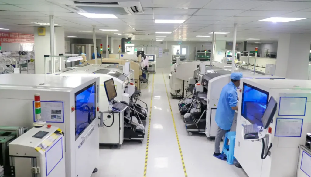
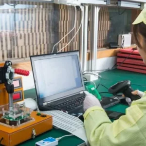
If you work in electronics manufacturing, sourcing, or product development, you have probably seen the term SMT in quotations, capability sheets, assembly drawings, and PCB documentation. SMT stands for Surface Mount Technology. It is the standard method of mounting electronic components directly onto the surface of a printed circuit board instead of inserting leads through drilled holes. In modern electronics, SMT is the dominant assembly approach because it supports compact layouts, automated production, and high component density.
For engineers, SMT affects footprint design, stencil strategy, placement accuracy, reflow performance, and test planning. For procurement teams, SMT affects supplier capability, quality risk, lead time, compliance documentation, and total project cost. That is why understanding the meaning of SMT is useful—but not enough on its own. In practice, buyers also need to know how the process works, what standards matter, and what files should be prepared before requesting a PCBA quotation.
This guide explains SMT from a practical B2B perspective: what SMT means, how it differs from SMD and through-hole assembly, what happens in a typical SMT production flow, which IPC and compliance requirements buyers commonly ask about, and what data a supplier needs to quote and build a board correctly the first time.
SMT Meaning
Definition: Surface Mount Technology (SMT)
Surface Mount Technology (SMT) is a PCB assembly method in which electronic components are mounted directly onto pads on the board surface and then soldered, typically using a reflow process. The components used in this method are called Surface Mount Devices (SMDs). Compared with traditional through-hole assembly, SMT enables smaller product size, more automated production, and double-sided component placement.
Why SMT Matters for PCBA Buyers
For OEMs, engineers, and procurement teams, SMT matters because it directly affects manufacturability, product size, cost structure, and production efficiency. SMT supports higher component density, more consistent automated placement, and scalable output from prototype to volume production. It also makes it easier to build complex boards with mixed passive and IC populations on one or both sides of the PCB.
From a buying perspective, a capable SMT supplier should do more than just place parts. They should be able to review design risks, confirm whether the board fits their process window, define inspection and test coverage, and tell you exactly what information is needed to avoid quotation errors or production delays. That is where a good SMT partner adds value beyond unit price.
SMT vs SMD vs Through-Hole (THT): What’s the Difference?
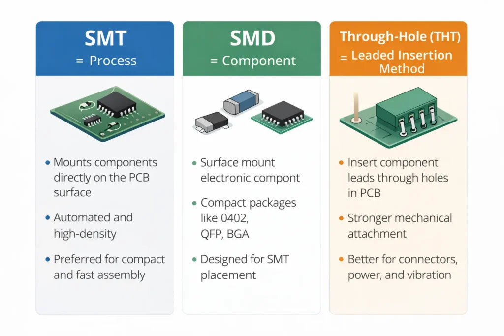
SMT (Process) vs SMD (Component)
These two terms are related, but not interchangeable.
SMT refers to the assembly technology or manufacturing process
SMD refers to the component itself, such as chip resistors, capacitors, QFPs, QFNs, BGAs, and similar packages designed for surface mounting.
A simple way to explain it is this:
you use SMDs in an SMT process.
This distinction matters in real communication with suppliers. Buyers may ask about SMT capability, such as fine-pitch placement, BGA handling, or reflow profile control. At the same time, the BOM lists the actual SMD packages that must be sourced and assembled. Keeping the terms clear helps reduce misunderstanding during quotation and engineering review.
When Through-Hole Still Makes Sense
Although SMT is now the standard for most modern electronics, through-hole technology (THT) is still the right choice in specific scenarios. Through-hole parts remain useful where strong mechanical anchoring, large solder volume, or high insertion force is required.
Typical examples include:
connectors exposed to repeated mating cycles
transformers, relays, and other bulky parts
high-power components that benefit from stronger leaded attachment
products used in vibration-prone or mechanically stressed environments.
This is why many practical products use mixed assembly rather than pure SMT or pure THT. SMT handles compact and dense signal circuitry efficiently, while THT is reserved for parts that require mechanical or thermal robustness.
Mixed Assembly Decision Checklist
Before finalizing your board and supplier selection, ask:
Which parts truly require through-hole for strength or power handling?
Can the board be assembled in one supplier using both SMT and THT?
Will wave soldering, selective soldering, or manual insertion be required?
Are inspection and rework access still practical after the full assembly sequence?
These questions are especially important for industrial, power, communication, and instrumentation products where mixed technology is common.
Main SMT Assembly Process
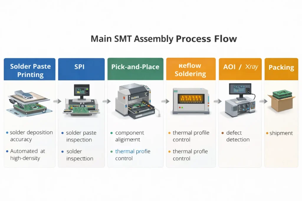
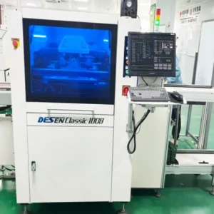
Step 1 — Solder Paste Printing
The SMT flow usually starts with solder paste printing. A stencil is aligned over the PCB, and solder paste is deposited onto the pads where components will be placed. This step is critical because solder volume and alignment directly influence downstream defects. Too much paste can cause bridging; too little can create insufficient solder joints or opens; poor alignment can contribute to skew, tombstoning, or reflow instability.
In most production environments, stencil design, aperture geometry, paste condition, board support, and printing parameters all matter. For boards with fine-pitch ICs, bottom-terminated packages, or mixed package sizes, printing quality is often one of the biggest determinants of overall SMT yield.
Many suppliers also use SPI (Solder Paste Inspection) after printing to verify paste height, area, and volume before the board moves to placement. For buyers, this is an important quality signal: it shows the supplier is not relying only on final inspection to catch defects.
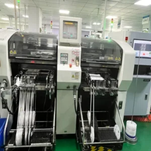
Step 2 — Pick-and-Place
Once paste is printed, the board moves to the pick-and-place stage. Automated placement equipment picks up SMDs from feeders, aligns them using vision systems, and positions them on the paste deposits.
At this stage, supplier capability matters in practical ways:
minimum package size they can place reliably
fine-pitch accuracy
BGA and QFN experience
feeder setup discipline
handling of polarity-sensitive or moisture-sensitive components.
For quoting and programming, suppliers usually need a centroid / pick-and-place file with X-Y coordinates, rotation, and layer assignment. Missing or inconsistent placement data slows engineering review and can increase NPI risk.
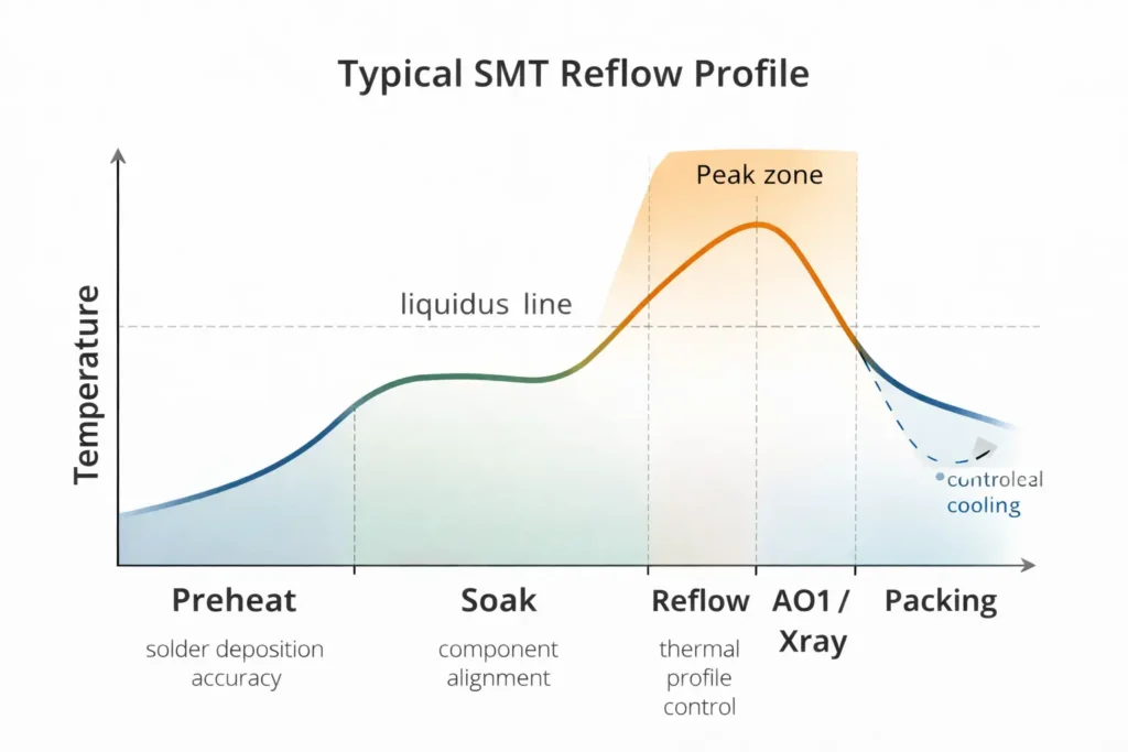
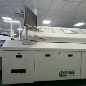
Step 3 — Reflow Soldering
After placement, the PCB enters a reflow oven. A standard SMT reflow process is commonly described in four thermal stages:
Preheat – gradually raises board temperature and reduces thermal shock
Soak – stabilizes temperature and supports flux activation
Reflow – takes solder above liquidus so joints form properly
Cooling – solidifies the solder joints in a controlled way.
Good reflow performance depends on more than oven temperature alone. Board mass, copper balance, component mix, solder alloy, and package sensitivity all affect profile optimization. A dense industrial control board and a lightweight consumer module do not behave the same way thermally.
This is one reason why serious suppliers document profile control, especially on new products, fine-pitch assemblies, or boards with thermal imbalance. For buyers, reflow control is not an abstract technical detail—it is directly related to solder joint reliability and first-pass yield.
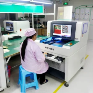
Inspection & Quality Gates
A robust SMT process includes inspection throughout production rather than only at the end.
Common inspection methods include:
SPI for solder paste verification
AOI for visible solder and placement defects
X-ray for hidden joints such as BGA and some bottom-terminated packages
First Article Inspection (FAI) before full production release.
AOI helps detect missing parts, polarity reversal, visible solder issues, and placement shifts. X-ray is essential where optical inspection cannot see the actual solder interface. For buyers handling BGA-heavy, high-density, or reliability-sensitive products, asking whether X-ray is available is often more meaningful than asking generic questions about “strict quality control.”
Electrical Test Options (ICT / FCT) & What Buyers Should Specify
After assembly and visual/structural inspection, many products also require electrical verification.
ICT (In-Circuit Test) is used to check shorts, opens, and component-level electrical conditions
FCT (Functional Circuit Test) powers the board and verifies that it behaves correctly in its intended operating mode
Buyers should specify, early in the RFQ stage, whether the project requires ICT, FCT, programming, firmware loading, fixture support, or customer-defined pass/fail criteria. Waiting until production starts often causes delay, fixture redesign, or avoidable miscommunication.

Design & DFM Tips That Directly Impact SMT Yield
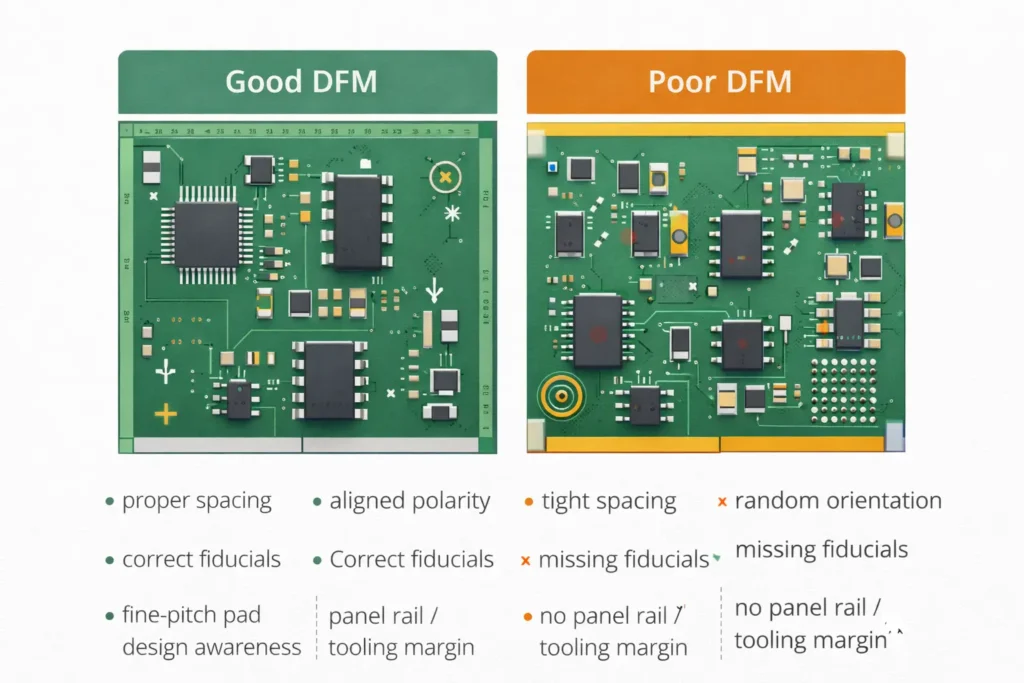
Footprint / Land Pattern: Why IPC-7351 Matters
SMT yield starts long before the board reaches the line. It begins with footprint and land pattern design.
A major reference in this area is IPC-7351, which covers generic requirements for surface-mount design and land pattern geometry. In practical terms, this standard is important because pad size, toe/heel length, spacing, and density choices all affect solder joint formation, placement stability, and manufacturability.
Poor footprint design increases the risk of:
solder bridging
insufficient wetting
tombstoning
component shift
inconsistent rework behavior
For most commercial and industrial projects, engineers should not design footprints in isolation from the intended manufacturing process. The best results come when land pattern decisions are aligned with stencil strategy, package type, and real supplier capability.
Spacing, Orientation, and Assembly Constraints
Good SMT design also depends on practical layout discipline.
Examples include:
leaving enough spacing for placement nozzles, inspection, and rework
keeping polarized parts consistently oriented for easier verification
avoiding random IC orientation when standardization improves programming and inspection
separating heat-sensitive parts from components with high thermal mass where possible
These design choices may look minor in CAD, but they affect programming efficiency, AOI performance, defect escape risk, and engineering clarity during NPI.
Stencil Considerations
Stencil strategy directly affects solder paste volume. Boards with mixed component sizes often create a tradeoff between large pads that need more paste and fine-pitch pads that need tighter control. In those cases, aperture optimization—or in more complex products, a step stencil—may be needed.
Buyers do not need to specify stencil engineering in full detail, but they should understand that very fine-pitch components, 0201/01005 passives, large thermal pads, and mixed-technology boards may require extra review. This is exactly the kind of DFM input a qualified supplier should raise before production.
Panelization and Fiducials: What to Include in Your Files
To support stable automated assembly, production data should include clear panel information and fiducial references where appropriate. Fiducials help placement systems align boards accurately, while good panelization improves handling, throughput, and process consistency.
At quotation and engineering review stage, it helps to provide:
panel drawing if the board is panelized
tooling and breakaway notes if needed
fiducial information for fine-pitch work
assembly notes for special handling or secondary operations
Quality Standards & Compliance Buyers Ask For
IPC Classes (Class 1 / 2 / 3) — How to Choose
In PCB assembly, buyers often refer to IPC Class 1, 2, and 3. These classes broadly reflect different levels of reliability expectation and acceptance rigor. Class 1 is associated with general electronics, Class 2 with dedicated service electronics, and Class 3 with higher-reliability applications where failure carries greater consequences.
In practice:
Class 2 is the most common baseline for many industrial and commercial products
Class 3 is more relevant for critical-use environments, higher-reliability systems, or projects with stricter workmanship and inspection expectations
The key point for buyers is this: the required class should be explicitly agreed. It should not be assumed.
J-STD-001 vs IPC-A-610 (Process vs Acceptability)
These two standards are often mentioned together, but they serve different roles.
J-STD-001 focuses on materials, methods, process requirements, and verification criteria for soldered assemblies
IPC-A-610 focuses on the acceptability of finished electronic assemblies, especially visual and workmanship criteria.
A simple way to explain the difference is:
J-STD-001 helps define how reliable soldering should be achieved
IPC-A-610 helps define whether the finished board is acceptable
For procurement teams, this matters because discussions about inspection standards, workmanship, and reject criteria often become vague unless these references are stated clearly in the order or quality agreement.
RoHS & REACH: What a PCB / PCBA Supplier Can Provide
For overseas B2B buyers, environmental compliance is often part of supplier qualification.
The European Commission describes RoHS as the EU framework restricting hazardous substances in electrical and electronic equipment. The RoHS scope currently covers ten restricted substances, including four phthalates added through later amendment.
REACH is the EU’s main regulation for managing chemical risks and protecting human health and the environment from substances of concern. In electronics projects, REACH questions often relate to material disclosure, SVHC communication, and supply chain transparency.
A practical PCB/PCBA supplier should be able to support buyers with documents such as:
RoHS compliance declarations
REACH statements or SVHC-related communication where applicable
material-level compliance information for sourced parts and assembly materials
For buyers in Europe—and often also in the US and Australia when serving global OEM supply chains—this documentation is not optional background material. It is often part of vendor approval.
RFQ Checklist: Files You Need for a Fast SMT PCBA Quote
Must-Have Files
To quote an SMT PCBA project accurately and quickly, suppliers usually need the following:
Gerber or ODB++ files
BOM with manufacturer part numbers, descriptions, quantities, and approved alternates
Centroid / pick-and-place file
Assembly drawing showing reference designators, polarity, and orientation notes
Testing requirements if ICT, FCT, or programming is required
Firmware / programming files where applicable
Substitution rules for sourcing flexibility
Special process notes, such as conformal coating, selective soldering, cleaning, or packaging requirements.
Providing a full RFQ package improves more than quote speed. It also reduces the chance of engineering assumptions, sourcing errors, or production delays later.
Nice-to-Have
These files are not always mandatory, but they often help:
3D files for mechanical fit review
panel drawing or panelization notes
solder mask opening notes for unusual pad conditions
test fixture interface details
approved AVL or alternate part guidance
reliability or environmental test requirements for regulated applications
Downloadable Templates
This is where your content can move from informational traffic to real conversion value.
A strong CTA at this point is to offer:
a BOM template
a PCBA RFQ checklist
optionally a DFM review request form
These resources help engineers and buyers get organized while naturally leading them into quotation or technical review. That is exactly the kind of useful, task-oriented content Google tends to reward over thin glossary-style pages.
FAQ
What is the main difference between SMT and THT?
SMT mounts parts directly on the PCB surface, while THT inserts leads through holes. SMT is usually better for compact, automated, high-density boards; THT is still useful for mechanically stressed or high-power parts.
Is SMT always cheaper than through-hole assembly?
Not always. SMT often reduces labor and improves automation, but total cost still depends on board complexity, package mix, inspection requirements, testing scope, and whether mixed assembly is needed.
What standards should I mention in a PCBA RFQ?
A practical starting point is to specify the required IPC class and confirm whether acceptance/process expectations will reference IPC-A-610 and J-STD-001.
Can one supplier handle both SMT and through-hole assembly?
Yes, many full-service EMS providers support both, but buyers should still confirm selective soldering, manual insertion, mixed assembly flow, and test capability before ordering.
What files are essential for a fast SMT quote?
At minimum: fabrication data, BOM, centroid file, assembly drawing, and any test or compliance requirements. The more complete your RFQ package, the more accurate the quotation.
Final Thoughts
At a basic level, SMT means Surface Mount Technology. But in real PCB assembly sourcing, SMT means much more than a definition. It affects design decisions, quality control, inspection methods, compliance requirements, and how smoothly your project moves from RFQ to shipment.
For engineers and procurement teams, the best supplier is not simply the lowest bidder. It is the supplier that can explain the process clearly, identify manufacturability risks early, align workmanship to recognized standards, and guide you on exactly what data is needed to build the board correctly the first time. That is also what your article should demonstrate to visitors—and this is where a strong B2B SEO page becomes a lead-generation asset instead of just a glossary entry.