Table of Contents
SMT vs THT: What’s the Difference?
SMT (surface-mount) places components directly onto pads on the PCB surface and solders them mainly with reflow, making it ideal for high automation, high density, high-speed signals, and scalable volume production.
THT (through-hole) inserts leaded components through drilled holes and solders them (often with wave or selective solder), which is still preferred for high mechanical stress parts (connectors, heavy components), some high-power/thermal needs, and easier field repair.
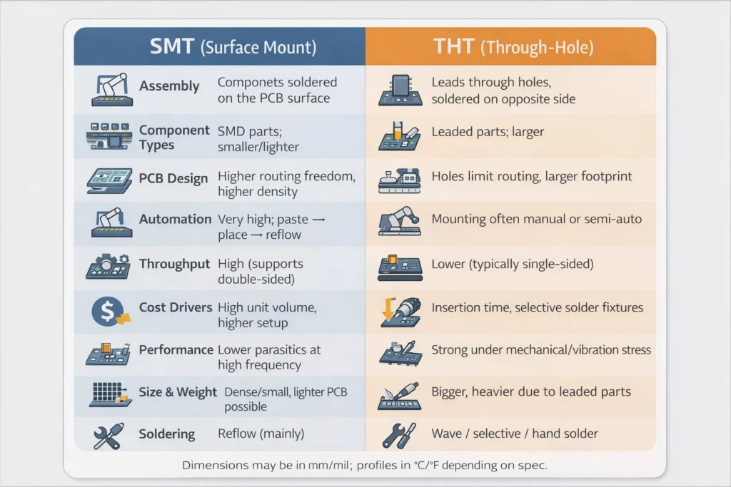
SMT vs THT comparison table
| Comparison dimension | SMT (Surface Mount) | THT (Through-Hole) |
|---|---|---|
| Assembly method | Components soldered on the PCB surface | Leads go through holes and are soldered on the opposite side |
| Component types | SMD parts (chip passives, QFN/QFP/BGA, etc.), typically smaller/lighter | Leaded parts (electrolytic caps, connectors, relays, pots), typically larger |
| PCB design impact | Fewer holes for parts → more routing freedom and higher density | Holes consume routing area; constrains dense layouts |
| Automation | Very high (paste print → place → reflow) | Lower overall; insertion may be manual/semi-auto; wave/selective can be automated |
| Throughput | Very high, supports double-sided assembly | Lower; insertion and solder steps add time |
| Cost drivers | Strong cost efficiency at scale; higher NRE/setup (stencil, programming) | Higher labor/touch time; fixtures and selective solder programming can add cost |
| Performance & reliability (typical) | Excellent high-frequency behavior; strong when footprints + process controls are right | Strong mechanical anchoring; often favored for high-stress connectors/heavy parts |
| Size & weight | Enables smaller/lighter designs via higher density | Larger footprint due to leaded parts and hole constraints |
| Soldering | Reflow (primarily) | Wave / selective / hand solder |
| Rework & service | Harder (fine pitch, hidden joints like QFN/BGA) | Easier to hand-rework and replace |
At a glance: SMT wins on density and automation; THT wins on mechanical anchoring and serviceability.
Definitions and Key Terms
What is SMT (Surface Mount Technology)?
SMT is a PCB assembly method where components are attached and connected on the surface of the board, typically using batch solder-reflow processes.
You’ll also see SMD (surface-mount device) used for the components themselves.
What is THT / PTH (Through-Hole / Plated Through-Hole)?
THT is a mounting method where component leads are inserted into holes drilled in the PCB and soldered on the opposite side.
PTH (plated through-hole) means the hole wall is plated (typically copper) to create electrical interconnect between layers—critical for multilayer boards.
How Each Assembly Process Works (step-by-step)
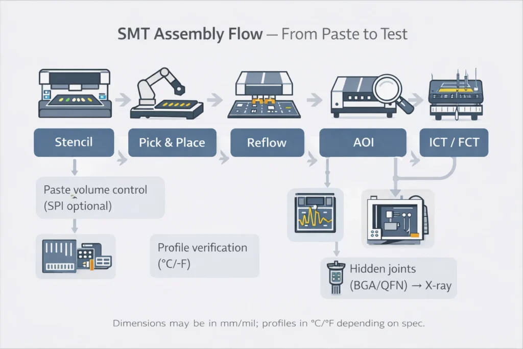
SMT process flow
Solder paste printing (stencil + printer)
Pick-and-place (place SMDs to pads)
Reflow soldering (controlled temperature profile in °C/°F equivalent profile settings)
Inspection (often AOI; X-ray for hidden joints; plus electrical test)
Suggested visual (flowchart): Paste print → Placement → Reflow → AOI/X-ray → ICT/FCT → Final inspection/pack.
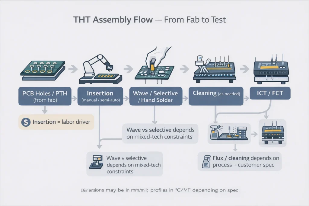
THT process flow
Drilling + plating happens during PCB fabrication (PTH creation)
Component insertion (manual or insertion equipment)
Soldering (wave / selective / hand)
Cleaning + inspection + electrical test (depending on flux/process/quality requirements)
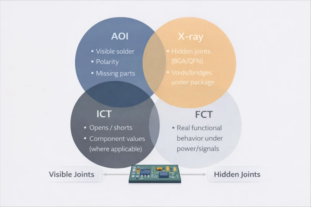
Where inspection fits: AOI, X-ray, ICT/FCT
AOI (Automated Optical Inspection): camera-based inspection during/after assembly for missing/wrong parts, polarity, solder appearance, etc.
X-ray inspection (AXI): used when joints aren’t visually accessible (common for BGA/QFN).
ICT (In-Circuit Test) & FCT (Functional Test): electrical verification—ICT focuses on nets/components; FCT validates real operating behavior.
Suggested visual: A simple “defect coverage map” showing what AOI vs X-ray vs ICT vs FCT can/can’t see.
Performance Differences That Matter in Real Products
Mechanical strength & vibration: connectors, heavy parts, and cable strain
THT has an inherent advantage when the product sees high vibration, shock, cable strain, or repeated mating cycles, because leads pass through the board and create a strong mechanical anchor. SMT joints rely on surface pads and solder fillets; they can be very reliable, but high mechanical loading needs careful design and reinforcement.
Electrical & thermal considerations: high-current paths, heat dissipation, creepage/clearance
THT is often favored for heavy copper leads, high-stress connectors, transformers, and some power parts, where mechanical anchoring and heat conduction paths matter. SMT typically excels in high-frequency/high-speed behavior because interconnects are shorter, reducing parasitics.
Serviceability & rework: field repair, replacement, and rework risk
THT is usually simpler to rework with common tools. SMT rework can be complex—especially for dense boards and hidden joints—so design-for-rework and the right rework equipment become important.
Miniaturization & signal integrity: why SMT enables higher density and shorter interconnects
SMT enables higher placement density (including both sides), which supports smaller products and better signal integrity in many high-speed designs.
Cost, Lead Time, and Scalability
SMT cost drivers: stencil, machine programming, placement count, package types
SMT cost typically scales with:
Placement count (how many parts must be placed)
Package complexity (fine pitch, BGA/QFN handling, special materials)
NRE/setup (stencil, programming, line setup)
Process requirements (lead-free profile, tighter inspection/test coverage)
Cost-down levers that usually work: consolidate passives, avoid unnecessary package variety, panelize smartly, and keep footprints IPC-compatible.
THT cost drivers: manual touch time, selective solder programming, fixtures, component availability
THT cost often comes from:
Insertion labor/touch time
Selective solder programming (when wave isn’t suitable)
Fixtures and masking
Supply chain constraints for certain leaded parts
Lead-time reality: NPI vs mass production
NPI builds tend to take longer because of setup, DFM loops, test strategy, and first-article validation.
In volume, lead time is dominated by parts availability, factory capacity, and test throughput.
When THT increases total cost even if parts look “simple”
Even a small number of THT parts can increase total cost by:
breaking continuous SMT flow (extra steps, WIP, scheduling),
increasing process risk (thermal exposure during wave/selective),
adding fixtures/masking and extra inspection.
Design for Manufacturability (DFM) Checklist
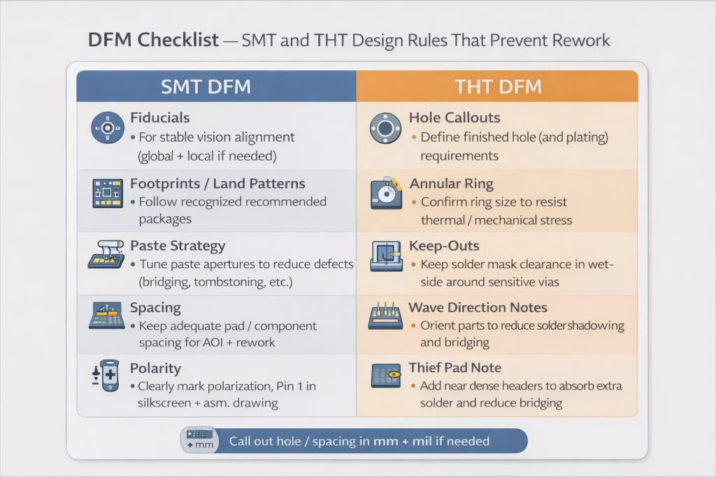
SMT DFM essentials: fiducials, paste rules, spacing, polarity, thermal balance
Fiducials: include global (and local when needed) fiducials for stable vision alignment.
Footprints/land patterns: follow a recognized land-pattern standard so solder joints are inspectable and reworkable.
Paste + pad strategy: tune paste apertures to prevent bridging/tombstoning; avoid “one-size-fits-all.”
Spacing: keep adequate clearance for placement, AOI visibility, and rework access (mm and mil conventions should be consistent in the fab/assy drawings).
Polarity marking: make polarity and Pin-1 unmistakable on silkscreen + assembly drawing.
Thermal balance: manage uneven copper/thermal mass to reduce tombstoning and insufficient wetting.
THT DFM essentials: hole sizing/tolerances, annular ring, keep-outs, wave orientation
Hole design: define finished hole requirements and plating intent (PTH vs NPTH) clearly; PTH is fundamental for multilayer interconnect.
Annular ring: ensure adequate annular ring for mechanical robustness, especially under thermal/mechanical stress.
Wave solder keep-outs: maintain solder mask clearance and component keep-outs on the wave side to reduce bridging and solder contamination.
Wave direction strategy: align layouts to reduce shadowing and bridging; add steal/thief pads where appropriate (document it in the assembly drawing).
Mixed-tech boards: layout tips to reduce hand-solder and improve yield
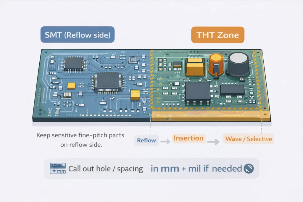
Plan the board so SMT and THT steps don’t fight each other:
keep most SMT on the reflow side,
isolate wave-side SMDs and protect when required,
reserve keep-outs around through-hole joints to avoid thermal/mechanical interference.
Testability: designing for ICT/FCT, test pads, and programming access
Add test pads for power/ground and critical signals (call out pad size/spacing in mm and mil if your EMS requests it).
Keep pads accessible (no tall parts blocking probes).
Plan programming access (JTAG/SWD/UART/USB) and confirm the fixture concept early.
Typical Applications
When SMT is the default choice
Consumer electronics
Computing/communications hardware
Dense industrial controls and instrumentation
When THT is still preferred
Power supplies and magnetics
High-stress connectors and frequently mated interfaces
Rugged equipment with high vibration/impact exposure
The most common scenario: SMT + THT on one board
A common flow is SMT first (reflow), then THT insertion, then wave or selective solder—with layout rules to protect sensitive SMT parts and reduce rework.
Common Defects and How Good Factories Prevent Them
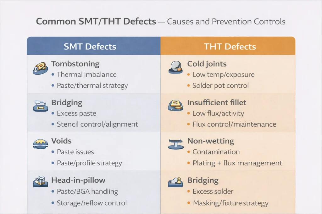
SMT defects: tombstoning, solder bridging, voiding, head-in-pillow
Tombstoning: often from thermal imbalance or uneven wetting; mitigated by pad/paste tuning + balanced thermal design.
Bridging: often from excessive paste, tight pitch, misalignment; mitigated by stencil design, placement accuracy, and footprint discipline.
Voids / head-in-pillow: mitigated via paste control, storage/handling, and verified reflow profiling.
THT defects: cold joints, insufficient fillet, pin non-wetting, bridging
- Typically controlled through solder pot parameters, flux control, conveyor speed, and cleanliness/wettability management.
Process controls that matter: SPI, reflow profiling, solder pot control
SPI helps catch paste volume/offset issues early.
Reflow profiling verifies real thermal behavior on the PCB.
Wave/selective solder control (temperature, alloy condition, contamination) is critical for stable through-hole joints.
How to Choose: A Practical Decision Framework
Use SMT if you prioritize
Miniaturization and high density
High automation and volume scalability
High-speed / high-frequency performance
Fine-pitch and advanced packages (QFN/BGA/CSP)
Use THT if you prioritize
Mechanical robustness (shock/vibration/mating cycles)
High current / power parts and heavy components
Field service and simpler replacement
Questions to answer before you lock the method
What’s the top requirement: size or ruggedness?
Does the BOM include parts that are effectively THT (connectors, large caps, magnetics)?
What environment: vibration, shock, thermal cycling, frequent plug/unplug?
What volume: prototype/NPI vs sustained mass production?
What reliability class and inspection/test coverage do you need?
If you’re unsure, send your BOM + mechanical constraints + expected environment. PCBAgroup can recommend a mixed-tech approach that reduces hand-solder and improves yield—without forcing a redesign.
What to Send for an Accurate PCBA Quote
Required files
Fabrication data: Gerber / ODB++ / IPC-2581
BOM (with manufacturer part numbers)
Pick-and-place / centroid file (for SMT)
Assembly drawing (polarity, refdes, special notes)
Programming/test notes (ICT/FCT requirements)
Tell PCBA Marufacturer
- Define acceptance criteria and workmanship expectations. IPC acceptance and soldering requirements are commoquality plans.
- If you use IPC product classes, align inspection with the class expectations.
- Specify conformal coating, potting, or environmental requirements upfront.
Common quote blockers
Incomplete files or wrong revisions
Unclear quantities/variants
Missing test strategy or programming access requirements
Unstated special processes (coating, selective solder constraints, special finishes like ENIG
FAQs
Is THT more reliable than SMT?
Not universally. THT is often stronger under mechanical stress, while SMT can be extremely reliable when footprints and process controls are correct. Reliability is a system outcome (design + process + environment), not just a mounting style.
Is SMT always cheaper than THT?
In volume, SMT is often more cost-effective due to automation. THT can become expensive because of insertion labor and extra solder steps. But a few THT connectors or power parts may still be the best engineering choice.
Can a board be both SMT and THT?
Yes—mixed technology is very common.
Wave solder vs selective solder—what’s the difference?
Wave solders many joints at once using a solder wave; selective targets specific joints for tighter control on mixed-tech boards.
What should I specify in an RFQ if my board has both SMT and THT?
Include the centroid file (SMT), clearly mark THT parts, and state soldering preferences (wave/selective/hand) plus inspection/testing requirements.
If you share Gerber/ODB++ + BOM + pick-and-place + assembly notes, we can respond with:
a short DFM risk list (SMT/THT hotspots, mixed-tech concerns),
recommended inspection/test options (AOI/X-ray/ICT/FCT),
and a quote plan aligned to your target volume and quality class.