Table of Contents
What Is a Rigid-Flex PCB?
Overview
A Rigid-Flex PCB integrates rigid sections and flexible sections into a single circuit board, with electrical interconnection achieved through continuous copper circuitry. In practice, rigid and flex zones are typically integrated through lamination and bonding processes (the exact process route depends on the stackup, structure, and supplier capability). This design maintains mechanical stability in rigid areas while leveraging the bending and folding capability of flex areas to fit complex internal packaging. In space-constrained products or applications with high reliability requirements, rigid-flex designs often enable more compact 3D packaging, and—when supported by proper design rules and process control—can improve interconnect robustness.
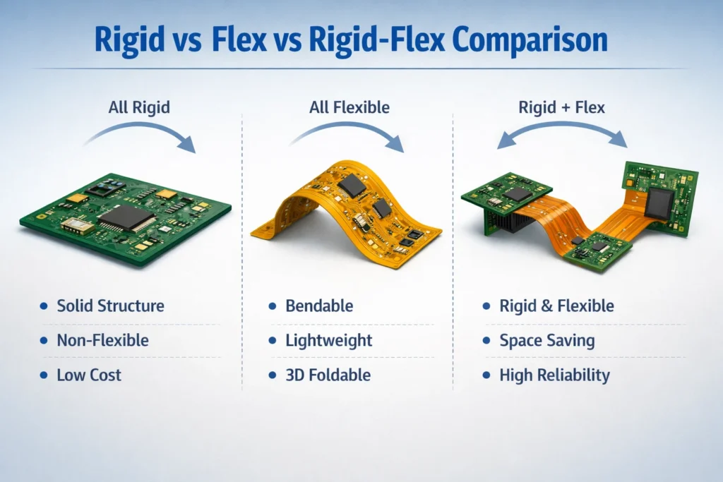
Rigid PCB vs Flex PCB vs Rigid-Flex PCB
| Attribute | Rigid PCB | Flex PCB (FPC) | Rigid-Flex PCB |
|---|---|---|---|
| Core structure | Fully rigid substrate | Fully flexible substrate | Hybrid rigid + flexible zones |
| Physical behavior | Strong, not bendable | Bendable, foldable; can support dynamic bending | Combines structural strength + bendability |
| Main advantages | Low cost, high stiffness, mature processes | Lightweight, thin, supports 3D routing, bendable | High integration density, space/weight savings, high reliability potential |
| Main limitations | Not bendable; limited flexibility for 3D/folded layouts | Lower standalone mechanical support; cost may rise with stiffeners/special finishes/high bend-life requirements | Higher unit cost; more complex design & manufacturing (depends on layer count, bending type, yield targets, and test requirements) |
| Typical applications | General consumer electronics, industrial control boards | Phone hinge areas, wearables, moving interconnects | High-end smartphones, medical devices (e.g., pacemakers), automotive, aerospace |
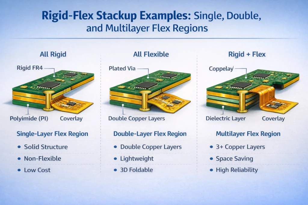
Common Rigid-Flex Stackup Types
Single-Layer Rigid-Flex
This is typically a relatively simple structure. The flex portion contains one conductive copper layer, usually sandwiched between two flexible dielectric layers such as polyimide (PI). This structure is often more achievable within standard supplier capabilities and cost frameworks, but routing density is limited. It is commonly used for simple interconnects, light bending, and low-to-mid-speed signals.
Double-Layer Rigid-Flex
In a double-layer flex zone, copper is present on both sides of the dielectric, and the layers are electrically connected through plated vias. This provides higher routing capability than single-layer designs and is relatively common in consumer and industrial products where moderate density is required.
Multilayer Rigid-Flex
Multilayer rigid-flex designs include three or more conductive layers in the flex region, separated by dielectric layers and interconnected with vias. This structure supports very high circuit density and complex signal routing, and is commonly used in applications demanding higher performance and reliability.
When Should You Choose a Rigid-Flex PCB?
| Selection Scenario | Core Benefit | Typical Applications | What You Gain (Practical Explanation) |
|---|---|---|---|
| Severe space + shape constraints | 3D routing, volume reduction | Smartphones, wearables, medical endoscopes, foldable hinge areas | Flex fits non-planar housings; rigid zones support components. Compared with rigid-only PCBs, rigid-flex makes 3D integration easier and improves layout freedom. |
| High reliability + durability requirement | Fewer interconnect points, better stress tolerance | Automotive, aerospace, industrial control, robot joints, gimbals | Replaces connectors/cables; fewer interconnects typically reduce connection-related failure risk. With correct bend-zone rules/materials/process matching, it performs better under vibration and mechanical stress. |
| Simplified assembly + system optimization | Potential reduction in system assembly complexity; improved SI potential | 5G modules, high-speed bus devices, volume consumer electronics | Reduces connectors/wire harness and solder steps; shortens interconnect path. Can reduce some impedance discontinuities and EMI sources (final SI depends on stackup/routing/return paths). |
| Dynamic bending + static support coexist | Multi-zone stackup: “dynamic vs static separation” | Foldable display driver circuits, foldable mainboards | Flex zone provides bend capability; rigid zones deliver stiffness for assembly, heat, and component stability. |
| Cost/process tradeoff is acceptable | Higher upfront cost; harder to repair | More common in products that value space + reliability | PI materials and precision lamination increase cost; design complexity and repair difficulty require evaluating alternatives. |
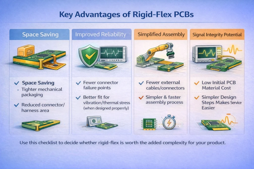
Key Advantages of Rigid-Flex PCBs
Space & Mechanical Packaging Benefits
Rigid-flex enables multiple rigid sections to be connected via a bendable flex section. This often reduces space occupied by internal wire harnesses/connectors and—when mechanical packaging is planned well—makes it easier to achieve a compact and lightweight internal structure.
Reliability Benefits
Higher Connection Robustness
A rigid-flex PCB replaces a system built from multiple connectors, cables, and interconnects. Fewer interconnect points typically reduce failures caused by contact issues, connector looseness, and interconnect fatigue, helping improve robustness in vibration/shock environments (overall reliability still depends on bend-zone design rules, materials, and process control).
Better Electrical Performance Potential
Reducing connectors/interposers can help reduce certain discontinuities and losses. In some high-speed/high-frequency applications, this can support better signal integrity—however the final result depends on stackup design, controlled impedance routing, and return path continuity.
Better Fit for Harsh Environments
Rigid-flex is often selected for environments involving vibration, temperature cycling, and mechanical stress. Real-world performance depends on design rules and verification.
Assembly & Lifecycle Cost Benefits
Simplified Assembly
When connectors, wire harnesses, and related soldering steps are reduced, assembly can often be simplified and consistency improved (actual impact depends on product assembly flow and fixtures).
Potential System-Level Cost Reduction
Although rigid-flex unit cost is usually higher, some projects can reduce system BOM, assembly labor, and maintenance risk by eliminating connectors/cables. A lifecycle cost evaluation is recommended.
Design Freedom & Functional Integration
Rigid-flex supports higher component density in limited space and enables multi-zone/multi-stackup designs. For example, heavy BGA components can be placed on thicker rigid zones for solderability/thermal needs, while thin flex zones support folding interconnects.
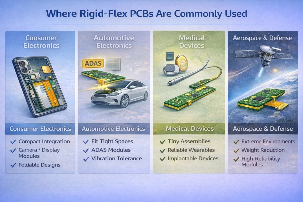
Common Applications of Rigid-Flex PCBs
Consumer Electronics
Smartphones & foldables: Commonly used in camera modules, display drivers, and power/battery management.
Wearables: Earbuds and smartwatches often use rigid-flex to replace wire harnesses for compact packaging.
Automotive Electronics
Used in ADAS modules, infotainment, instrument clusters, power management, and in-vehicle communications. Rigid-flex helps with compact packaging and can better tolerate automotive vibration/thermal conditions when designed and validated properly.
Medical Devices
Wearable medical devices: Conformal bending to body curves; resistance to movement/sweat environments.
Implantable devices: Very compact packaging with long-term reliability requirements.
High-end devices (endoscopes/surgical robots): High channel-count signals routed through narrow, bendable assemblies.
Aerospace & High-End Industrial
Used in applications requiring reliable interconnects under harsh conditions and weight constraints; industrial equipment may use rigid-flex to optimize thermal management and reduce noise/crosstalk in compact assemblies.
Rigid-Flex PCB Design Considerations
Structure Planning & Zone Definition
Multi-zone definition: Divide the PCB into physical zones on the XY plane. BGA/connectors are typically placed in rigid zones; fold/connection areas are defined as flex zones. Zones may be adjacent or nested but should not overlap. Undefined areas follow the primary stackup.
Multi-stackup mapping: Define appropriate stackups along the Z-axis for different zones. Rigid zones typically have more layers and thickness for mechanical support and dense routing; flex zones typically use fewer layers and thinner build-ups to maintain bendability. Stackups are mapped to zones to create a tailored “right stackup for each zone” design.
Mechanical Reliability Rules
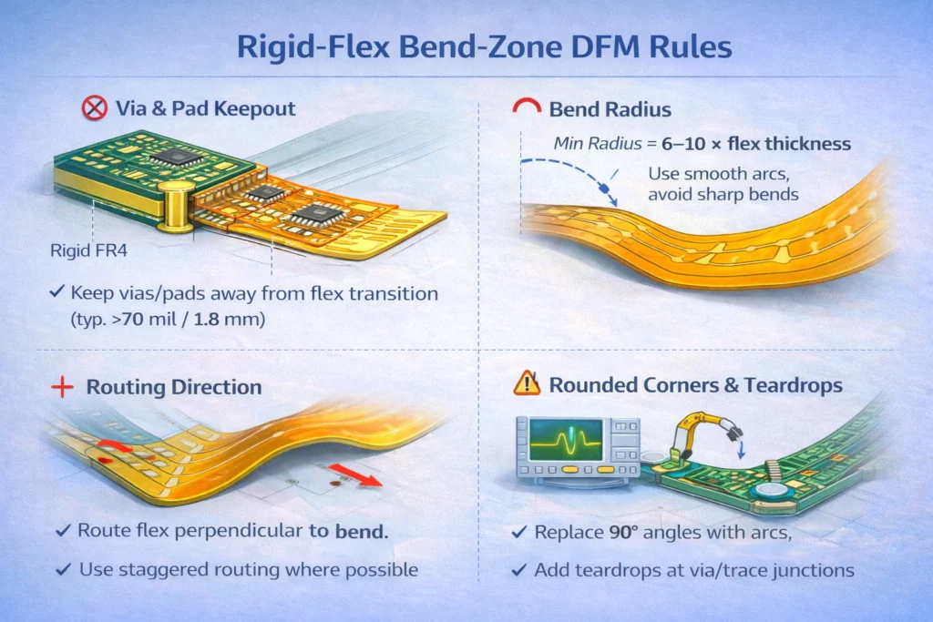
Bend-Zone Layout Rules
Via/Pad keepout: In dynamic bend zones, industry best practice is to strongly avoid vias, pads, and components because they create stress concentration and crack risk under repeated bending.
Transition clearance: Keep vias/pads/components away from rigid-flex transition edges.
Trace direction: In flex areas, routing is commonly oriented to reduce stress concentration; where possible, use routing patterns that distribute stress (often avoiding stacked overlap that increases thickness and local stress).
Geometry Optimization
Bend radius: Follow minimum bend radius guidelines to avoid excessive tensile strain (final radius depends on thickness, materials, and dynamic vs static bend conditions).
Rounded corners + teardrops: Use arcs or 45° transitions instead of right angles where possible. Add teardrops at trace-to-via connections to improve mechanical robustness and reduce copper peel risk.
Stiffener Strategy
Where components must be assembled on flex areas or connectors are inserted/extracted, stiffeners (FR4/PI/stainless steel) are commonly used to provide local rigidity and reduce deformation.
Material Selection
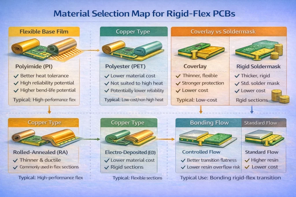
Flexible Base Material
Polyimide (PI) is commonly used due to good thermal performance and dimensional stability, supporting typical lead-free reflow processes (final ratings depend on material datasheets and validation standards). Polyester (PET) may be considered for lower-cost, lower-temperature applications. For high-density foldable designs, adhesiveless FCCL is often considered because it can be thinner and more flexible (selection depends on cost, yield, and reliability targets).
Conductor Material
Flex sections often use rolled-annealed (RA) copper for improved ductility and bend performance; rigid sections more commonly use electrodeposited (ED) copper for cost effectiveness.
Covering & Protection
Flex areas typically use polyimide coverlay (laminated film) for protection and flexibility. Rigid areas typically use liquid solder mask. EMI shielding layers may be added where needed.
Lamination / Bonding Materials
Many rigid-flex structures use controlled-flow bonding materials to reduce resin overflow into flex circuitry and improve transition flatness (the exact bonding system depends on stackup and supplier process).
Electrical & Thermal Design
Controlled Impedance & Signal Integrity
Because flex dielectrics and thickness differ from rigid regions, impedance calculation requires careful attention. Work with the manufacturer to calculate trace width/spacing based on selected material Dk/Df and stackup in order to meet targets (e.g., 50Ω single-ended, 100Ω differential) and maintain return path continuity.
Current Carrying Capability
Flex copper is often thinner. Line width should be calculated based on current and temperature rise targets. If needed, use local copper reinforcement, parallel routing, or structural changes.
Thermal Management
Place high-heat components in rigid zones where possible.
Use metal stiffeners as heat spreaders when required.
Consider CTE mismatch between rigid and flex materials and reduce thermal stress through design and process controls to prevent warpage/delamination.
Manufacturability & Assembly Readiness
DRC and Capability Alignment
Follow the manufacturer’s capability document for minimum trace/space, drill sizes, registration tolerances, and special processes.
Layer Registration
Flex materials can stretch during processing. Add sufficient optical targets/fiducials and consider stretch compensation.
Surface Finish
Rigid pads often use ENIG or HASL; flex pads commonly use OSP or soft gold plating depending on flexibility and reliability needs.
Assembly Considerations
Rigid zones should support reflow flatness; flex sections may require temporary fixation during assembly.
Rigid-Flex PCB Manufacturing Process
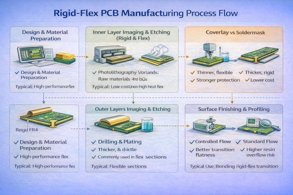
Design & material preparation
Inner layer imaging/etching (rigid & flex) + flex surface treatment for adhesion
Coverlay lamination & window opening (flex) — window accuracy affects lamination quality and transition flatness; some suppliers use advanced precision opening methods depending on design requirements
Lamination (rigid-flex bonding) — a key yield driver; precise alignment and resin-flow control are critical
Drilling + hole metallization
Outer layer imaging/etching
Surface finish + final profiling (laser/routing) and separation of flex areas
Electrical test & inspection (continuity, impedance as required)
Cost Drivers of Rigid-Flex PCBs
Material Costs
Flex core materials (FCCL): PI-based FCCL is expensive; better thermal stability often increases cost.
Bonding materials: Controlled-flow bonding materials are typically more expensive than standard FR-4 systems.
Coverlay & stiffeners: Additional protective films and stiffeners add cost.
Design & Process Complexity
Layer count & structural complexity: More layers and mixed rigid/flex constructions increase process steps and difficulty.
High precision requirements: Tight trace/space, microvias, and registration control raise manufacturing cost.
Yield and cycle time: Many steps and strict alignment/lamination control can reduce yield; deviations can cause misregistration, delamination, or scrap risk.
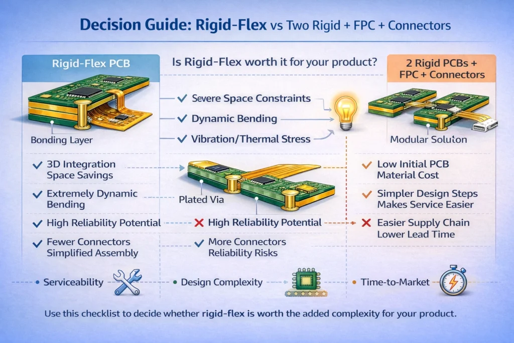
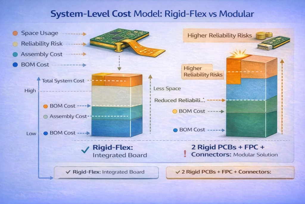
Rigid-Flex vs Two Rigid Boards + FPC + Connectors
| Attribute | Rigid-Flex PCB (Integrated) | 2 Rigid Boards + FPC + Connectors (Modular) |
|---|---|---|
| Form | Single integrated assembly | Multiple parts assembled |
| Biggest strength | Reliability potential, SI potential, extreme space saving, simplified integration | Lower initial materials cost, mature supply chain, easier modular repair |
| Main drawbacks | Higher manufacturing cost; complex design/production; longer lead time; harder to repair | More interconnect failure points; SI challenges; more space; higher assembly effort |
| Typical use | Foldables, aerospace, high-reliability medical, automotive ADAS, high vibration/shock areas | Cost-sensitive consumer electronics, fast-iteration prototypes, low-stress interconnect areas |
Order & Supply Chain Factors
Quantity: Higher volumes amortize NRE/engineering and reduce unit price; prototypes and low-volume runs cost more.
Lead time: Expedited delivery may add cost due to schedule disruption and extra control.
Material price volatility: Copper/glass/resin supply affects costs; rigid-flex is more processing-driven but material increases still impact total price.
Design file quality: Clear, accurate, capability-aligned files reduce rework and engineering iterations.
Practical Cost-Down Checklist
Route only the signals that must cross the flex region through flex layers to reduce flex layer count
Apply strict keepout rules in dynamic bend areas (avoid vias/pads/components)
Tighten tolerances only where necessary—avoid over-tightening globally
Lock the stackup and impedance targets before routing to avoid late-stage redesign
Choose surface finish and material systems based on real requirements (avoid “default premium”)
Perform DFM early (one pre-prototype correction beats a production rework)
Optimize panelization, profiling, and protection with the factory to reduce handling loss and shipping risk
RFQ
PCB Fabrication Files
Gerber or ODB++
Drill files (including drill table)
Target stackup, finished thickness, copper thickness requirements
Bend & Mechanical Files
Clearly mark bend areas, bend direction, fold shape
Static/dynamic bend definition and target bend radius
2D mechanical drawing + 3D/STEP (if available) or assembly illustration
Electrical & Reliability Requirements
Controlled impedance targets (e.g., 50Ω single-ended / 100Ω differential) and tolerance
Use environment (temperature, vibration, humidity) and reliability grade requirements
Test requirements: E-test, impedance test, microsectioning, special inspections (if needed)
If You Need PCBA
BOM (with MPN and alternates strategy)
Pick & Place file
Assembly drawing, stencil requirements, soldering process requirements
Programming / functional test instructions
If you’re planning a rigid-flex project and want to reduce risk early, contact PCBAgroup for stackup feasibility feedback, DFM suggestions, and a quotation based on your target reliability and manufacturing constraints.