Table of Contents
What Is a Flexible PCB? Definition, Types, Materials, Design Rules, Testing, and Cost
What Is a Flexible PCB (Flex Circuit / FPC)?
A Flexible Printed Circuit Board (also called a flex PCB, flex circuit, or FPC) is a printed circuit made on a flexible insulating film—most commonly polyimide (PI). Because it can bend, fold, and conform to complex 3D product shapes, flex PCB technology is a major enabler of miniaturization, lightweight design, and high integration in modern electronics.
Flexible PCB Definition
A flex PCB is a circuit patterned on a flexible dielectric film instead of rigid FR-4. Unlike rigid boards, a flex PCB is not limited to a fixed shape—it can be designed around the product’s mechanical structure to route signals and power through tight or curved spaces.
What makes a PCB “flexible”?
1) Core materials
Flexible base film (dielectric layer)
Polyimide (PI): Industry-standard for most flex PCBs due to heat resistance, dimensional stability, and mechanical strength. Well-suited for reflow soldering and repeated bending.
Polyester (PET): A lower-cost option for less demanding, lower-temperature applications.
Flexible conductor
The conductive layer is typically copper foil. For applications requiring higher bend reliability (especially dynamic flex), rolled-annealed (RA) copper is often preferred over electrodeposited (ED) copper.
Adhesives and protective layers
Layers are laminated using flexible adhesive systems (or built as adhesiveless stackups).
The outer surface is protected by coverlay (flexible PI film + adhesive) or sometimes flexible LPI solder mask (liquid photoimageable mask).
2) Lamination structure: the physical form that enables bending
A typical single-layer flex stack (bottom → top):
Flexible base film → adhesive → copper circuit layer → adhesive → coverlay
For more complex designs, double-sided or multilayer flex uses plated holes/vias to interconnect layers, while maintaining flexibility through careful material selection and process control.
3) Design for stress: static vs dynamic use
Flex PCBs can achieve long service life—even in motion applications—only if bend zones are designed correctly, including routing strategy, bend radius, via avoidance, reinforcement, and stress relief.
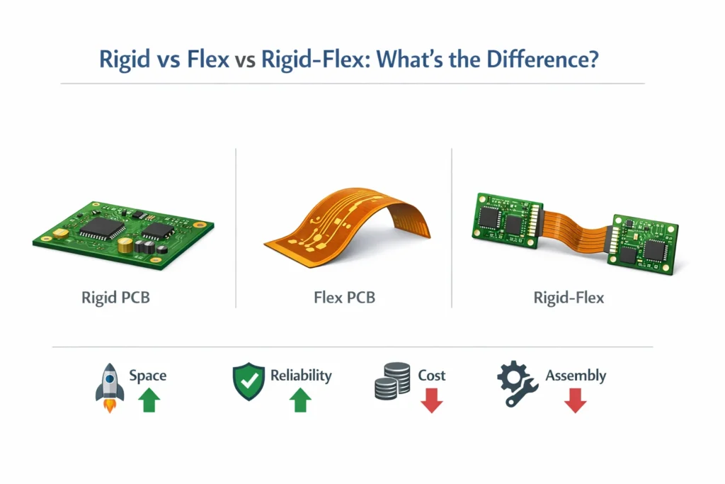
Flexible PCB vs Rigid PCB vs Rigid-Flex
| Type | What it is | Flexibility | Best for | Typical trade-offs |
|---|---|---|---|---|
| Rigid PCB | FR-4 fiberglass epoxy board | None | Cost-effective stable platforms | Cannot bend; bulkier interconnects |
| Flex PCB | PI/PET film-based circuit | High | Lightweight, compact interconnects | Higher unit cost than rigid; needs bend-zone DFM |
| Rigid-Flex | Rigid + flex integrated into one structure | Selective | Highest system reliability; fewer connectors | Higher cost; more complex design/fabrication |
Rule of thumb
If you’re replacing cables/connectors and need packaging freedom, flex is usually sufficient.
If you need multiple rigid component zones connected reliably in one integrated board, rigid-flex is often the best choice.
Why Use a Flexible PCB?
Save space and weight in compact products
Compared with rigid PCBs, flex circuits can significantly reduce product size and mass. They can bend, fold, or wrap through 3D spaces, allowing circuits to be embedded into irregular cavities.
Fewer connectors = higher reliability and easier assembly
Flex PCBs reduce dependence on connectors, harnesses, and intermediate solder joints. By integrating interconnects into one continuous substrate, they often:
simplify assembly
reduce handling errors
reduce failure points (connector fretting, intermittent contact, harness fatigue)
Enable folding, bending, and moving parts (static vs dynamic flex)
Static flex: bent during assembly and then fixed; not intended to move repeatedly.
Dynamic flex: bends repeatedly during product life (hinges, joints, sliding mechanisms). High cycle life is achievable only with correct materials + bend-zone design + validation testing.
Better packaging freedom for industrial design
Flex supports compact, ergonomic, and aesthetically smooth product shapes. When combined with rigid areas (rigid-flex), it enables high-density component loading while maintaining flexible interconnects.
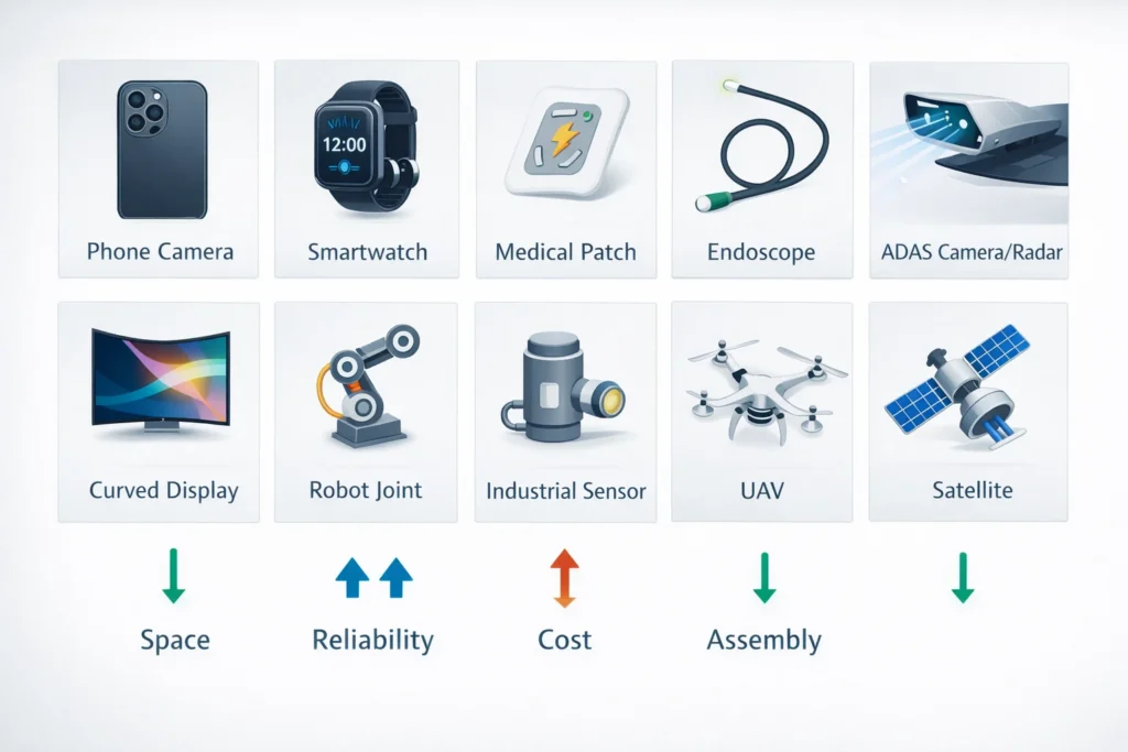
Common Applications of Flexible PCBs
Consumer electronics: camera modules, wearables, smartphones, foldables, laptops (hinge zones)
Medical devices: wearables, portable devices, endoscopes, implant-adjacent electronics (application dependent)
Automotive/transportation: ADAS sensors, infotainment displays, lighting modules (typically strict reliability requirements)
Industrial & robotics: moving joints, compact sensors, automation modules
Aerospace/defense: weight-sensitive, high-reliability systems (typically strict controls)
Flexible PCB Types and Structures
Single-sided flex
A basic construction with one copper layer, flexible base film, and protective coverlay. Best for simple routing and high flexibility at lower cost.
Double-sided flex
Copper on both sides, interconnected by plated through holes or vias. Enables higher routing density without increasing board area.
Multilayer flex
Three or more copper layers separated by flexible dielectrics, with interconnects via through/blind/buried vias. Supports higher density and controlled impedance, but increases complexity, cost, and bend-radius constraints.
Dynamic flex vs static flex
Key decision points:
expected bend location, angle, and frequency
required lifetime cycles (if dynamic)
stackup thickness and copper choice
whether adhesiveless construction is needed
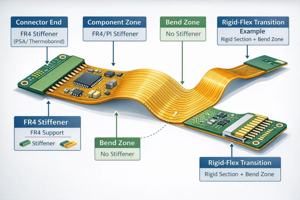
Stiffeners (FR4 / PI / Stainless / Aluminum) and when you need them
When stiffeners are needed
support heavy components or connectors
improve handling during SMT on very thin flex
reduce stress at rigid-to-flex transitions (including rigid-flex designs)
support ZIF connector mating areas
improve structural stability under vibration/shock
Common stiffener options
| Stiffener material | Typical purpose | Pros | Trade-offs |
|---|---|---|---|
| FR4 | SMT support, connector reinforcement | Cost-effective, widely available | Fully rigid; adds thickness |
| Polyimide (PI) | Moderate reinforcement | Similar mechanical behavior to flex | Less rigid than FR4 |
| Stainless steel | High mechanical stability | Very strong, durable | Higher cost and weight |
| Aluminum | Reinforcement + heat spreading | Good strength-to-weight; thermal benefit | Must manage electrical isolation |
Flexible PCB Materials Explained
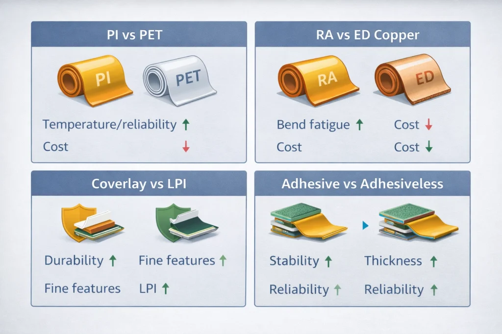
Base film: Polyimide (PI) vs PET
PI: Strong heat stability, compatible with standard reflow processes, good mechanical performance, chemical resistance, and long-term bend durability.
PET: Cost-driven alternative for lower-temperature, lower-mechanical-demand designs.
Copper foil: RA copper vs ED copper
RA copper: Produced by rolling and annealing; typically offers higher ductility and better bend fatigue behavior. Often chosen for dynamic flex or demanding bend zones.
ED copper: Electrochemically deposited; often higher tensile strength but typically lower ductility. More cost-effective and commonly used for many static flex builds.
Coverlay vs solder mask (LPI)
Coverlay: PI film + adhesive laminated onto the circuit; excellent mechanical protection and bend durability; openings are typically laser/tool cut.
Flexible LPI solder mask: thin photoimageable coating; cost-effective and supports fine features, but may crack in harsh dynamic bending conditions.
Adhesive-based vs adhesiveless stackups
Adhesive-based: simpler, lower cost; adhesive layer may reduce thermal/dimensional stability and can be a long-term reliability weak point in harsh conditions.
Adhesiveless: copper bonded without a separate adhesive layer; typically improves thermal stability, dimensional control, and can support thinner, more flexible builds.
Surface finishes for flex
| Finish | Why choose it | Watch-outs / notes |
|---|---|---|
| ENIG | Flat surface, oxidation resistance, good solderability; common for fine pitch | Higher cost; control process quality |
| OSP | Low cost, very flat, eco-friendly | Shorter shelf life; sensitive to handling/thermal cycles |
| Immersion Silver (IAg) | Excellent conductivity; good for high-speed/RF | Storage/environment control to prevent tarnish |
| Immersion Tin | Good solderability, competitive cost | Evaluate whisker risk for high-reliability designs |
| Selective Hard Gold | Best wear resistance for contact pads/gold fingers | Expensive; usually applied only to contact areas |
Flexible PCB Design Guidelines
Bend radius basics
Bend radius depends on:
total thickness
layer count
copper type and thickness
static vs dynamic usage
mechanical constraints of the product
Best practice: Define bend requirements clearly in drawings (bend line, direction, radius, static/dynamic) and confirm during DFM.
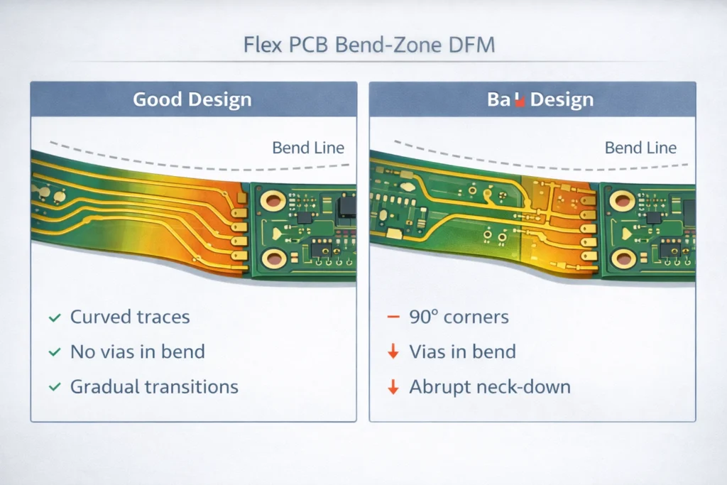
Routing in bend areas
In bend zones:
avoid sharp corners; use smooth curves and stress-relief features (fillets/teardrops where appropriate)
avoid sudden width changes; use tapered transitions
balance copper distribution to reduce localized stress and curling
keep critical features away from maximum strain regions
Vias and pads in flex
avoid plated holes/vias in dynamic bend zones when possible
do not place pads/components inside active bend zones
if unavoidable, work with the manufacturer to optimize structure and placement
Stiffener and reinforcement design
For connectors and high-stress zones:
specify stiffener material/thickness/location clearly
use mechanical support strategies to protect solder joints and pads
Signal integrity and EMI
Controlled impedance is achievable, but requires:
a clearly defined stackup (dielectric thickness control)
consistent fabrication processes
impedance targets and tolerances specified in the RFQ
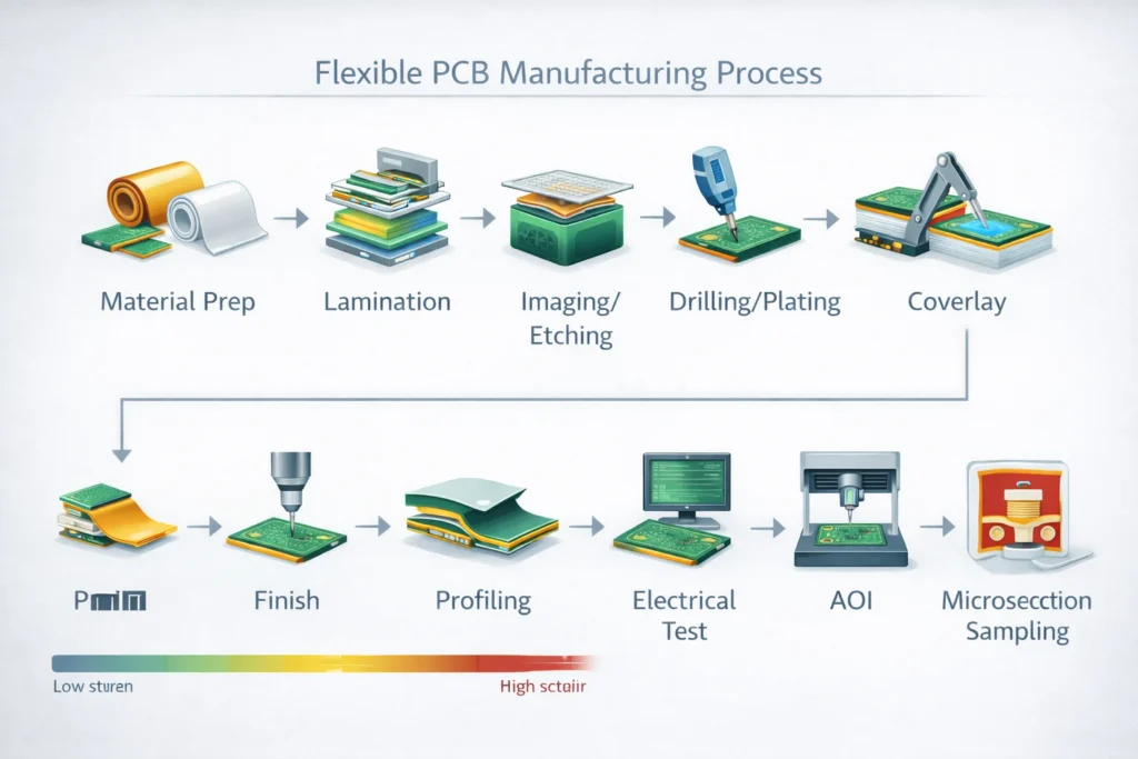
Typical Manufacturing Process for Flexible PCBs
Material preparation and lamination
Flex materials often come in rolls/sheets and are cut to panel size to reduce waste. Lamination typically uses:
Adhesive-based lamination: epoxy/acrylic adhesive bonds copper to base film
Adhesiveless construction: copper is bonded without a separate adhesive layer (e.g., seed layer + plating buildup or direct bonding methods)
Imaging/etching and plated through holes
Circuit pattern formation:
apply photoresist → UV expose with phototool → develop → etch → strip resist
For double-sided/multilayer:
mechanical or laser drilling for through/blind vias
chemical deposition + copper electroplating to metallize holes and build thickness
Coverlay application and curing
Coverlay (PI + adhesive) is aligned, laminated under controlled heat/pressure, and cured. Adhesive flow control is key to bonding strength and avoiding excess squeeze-out.
Surface finish and final profile
Surface finish protects exposed pads from oxidation and ensures solderability/contact performance. Final profiling options include:
steel rule die cutting (simple shapes, high volume)
laser cutting (complex outlines, prototypes/small batches)
routing (certain geometries)
Electrical test + inspection
Common controls include:
electrical test (flying probe or fixture)
AOI (with flex-appropriate fixturing)
microsection analysis (cross-section validation)
dimensional checks
bend endurance testing (for dynamic requirements)
peel strength testing (adhesion validation)
Quality, Reliability, and Testing
Common failure modes and how they’re prevented
Cracking (trace fatigue): Often occurs in repeated bend zones and can cause opens or intermittent connections.
Prevention: appropriate bend radius, avoid vias in bend zones, RA copper where needed, smooth routing, and strain relief.
Delamination: Separation between layers (copper/base film/coverlay), caused by poor lamination control, low adhesion, or excessive bending/thermal stress.
Prevention: qualified materials, controlled lamination, conservative bend design, and process inspection.
Pad lift / copper peel: Copper separates from the base film due to repeated stress or inadequate adhesion.
Prevention: adhesion control and testing, reinforcement for high-stress pads, and mechanical support around connectors/components.
Incoming and in-process controls
Ask about:
lot traceability and material certifications
thickness/size control at multiple steps
adhesion/peel strength verification
key process monitoring during lamination, drilling, plating, and coverlay application
Suggested tests based on use case
dynamic bend fatigue testing (if required)
thermal cycling and humidity testing for environmental durability
vibration testing (especially transportation/automotive)
salt fog (where corrosion risk is relevant)
insulation resistance / dielectric withstand where needed
IPC standards and acceptance criteria
Commonly referenced standards include:
IPC-2223 (flex/rigid-flex design guidance)
IPC-6013 (flex PCB qualification/performance)
IPC-A-600 (PCB acceptability)
IPC-A-610 (assembly acceptability)
IPC-TM-650 (test methods)
IPC-9257 (electrical test requirements)
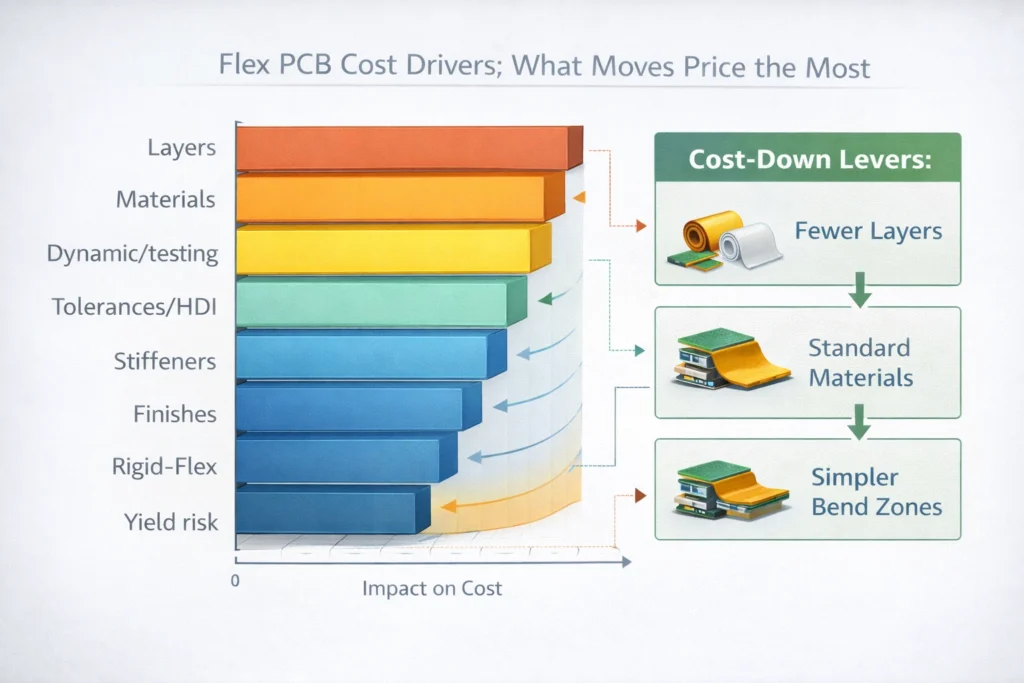
Flexible PCB Cost Drivers
What increases cost the most
layer count and design complexity (additional lamination, drilling, plating steps)
premium materials (PI, RA copper, adhesiveless stackups)
dynamic requirements and added reliability testing
tight tolerances, fine features, impedance control
complex rigid-flex transitions and precision alignment
specialized finishes or selective hard gold
yield loss risk with challenging geometries/process windows
Design choices that lower cost
simplify stackup and reduce layers where possible
improve panel utilization with manufacturable outlines
follow bend-zone rules to prevent expensive reliability failures
use standard materials/thicknesses when feasible
provide clear drawings/specs to reduce DFM iterations
Prototype vs mass production pricing logic
prototypes have higher unit cost due to one-time engineering/setup costs spread over small volume
production reduces unit cost through amortization, bulk procurement, stable process windows, and higher yield
Lead time: what affects delivery and how to avoid delays
Main drivers:
incomplete files/specs and slow DFM clarification
non-standard material sourcing
complex processes (rigid-flex alignment, laser drilling)
rework risk if bend requirements are unclear
Avoid delays by:
running DFM review early
standardizing materials where possible
submitting complete RFQ packages
clearly stating end-use, bend requirements, and reliability expectations
How to Request a Quote
Files to provide
Gerber or ODB++
stackup drawing (materials, copper thickness, final thickness)
fabrication notes + assembly drawing (if applicable)
mechanical drawing: outline, tolerances, bend zones, stiffeners
Critical specs to confirm
final thickness and tolerances
bend type (static/dynamic), bend line, direction, radius
impedance targets and tolerance (if needed)
surface finish
stiffener details (material, thickness, location, bonding method)
If you also need assembly
complete BOM (MPNs, package, qty, refdes)
pick-and-place file (XY, rotation, refdes)
test/programming requirements
for flex PCBA: consider functional testing after bending if the product bends in use
RFQ quick table
| RFQ item | Why it matters |
|---|---|
| Bend definition (static/dynamic, radius, location) | Determines materials, stackup, reliability risk |
| Stackup + final thickness | Impacts bend behavior, impedance, manufacturability |
| Finish and contact requirements | Affects solderability, wear resistance, storage |
| Stiffeners and bonding method | Critical for connector integrity and assembly yield |
| Test plan / acceptance criteria | Aligns supplier inspection with your risk level |
Flexible PCB vs Rigid-Flex
| Product constraint | Choose Flex PCB when… | Choose Rigid-Flex when… |
|---|---|---|
| Space & weight | You need ultra-thin/light interconnects that conform to 3D space | You need multiple rigid zones integrated into one compact structure |
| Reliability | You need good vibration/bending resistance with fewer connectors | You need maximum system reliability by eliminating connectors/cables |
| Assembly | You have limited rigid zones or can use gold fingers/ZIF | You want to remove board-to-board connectors and simplify assembly |
| Cost | You need lower upfront cost for simpler builds | Higher upfront cost but can reduce total system cost at scale (fewer parts, simpler assembly) |
When rigid-flex is worth it
Rigid-flex is often worth it when system reliability and connector reduction are top priorities, and you need multiple rigid component regions integrated in one design.
When standard flex is enough
Standard flex is usually enough when you mainly need a lightweight, compact interconnect and component loading is limited (or can be reinforced with stiffeners).
FAQ
How long can a flex PCB operate while bent?
It depends on bend radius, thickness, layer count, copper type, routing, and whether the application is static or dynamic. For dynamic use, define expected cycles and validate with testing.
What is the minimum bend radius for a flex PCB?
There is no universal number—it depends on stackup and use case. Specify bend requirements in drawings and confirm with DFM.
Is PI always better than PET?
PI is usually preferred for reflow assembly, high reliability, and harsh environments. PET can be suitable for cost-focused, low-temperature, less demanding designs.
RA copper vs ED copper—when should I choose RA copper?
RA copper is commonly used when bend fatigue performance is critical, especially in demanding bend zones or dynamic applications.
Coverlay vs flexible solder mask—what should I use?
Coverlay is typically preferred for bend durability and strong mechanical protection. Flexible solder mask can support thinner builds and fine features depending on reliability needs.
Work With a Flexible PCB Manufacturer
If your goal is fewer redesign cycles and higher reliability, the best next step is a DFM (Design for Manufacturability) review before production. A capable manufacturer can help you:
recommend an optimized stackup (PI/PET, RA/ED, coverlay/LPI, adhesive vs adhesiveless)
validate bend zones and stiffener strategy
reduce cost through panelization and manufacturability improvements
align inspection and testing to your application risk level
Ready for a quote?
Send your Gerber/ODB++, stackup, and mechanical drawings (bend line/radius + stiffeners). If you also need assembly, include BOM + pick-and-place + test requirements.