Table of Contents
High-Density Interconnect PCB : The Ultimate Guide for Engineers & Sourcing
High-Density Interconnect (HDI) PCBs enable smaller, lighter, and higher-performance electronics by using laser-drilled microvias, fine line/space routing, blind/buried vias, and sequential lamination. For engineers, HDI solves fanout and signal integrity constraints in modern packages (BGA/CSP). For procurement teams, HDI introduces new cost drivers (lamination cycles, via filling, LDI registration) that must be managed early through DFM collaboration.
This guide explains HDI definitions, stackups (1+N+1 to any-layer/ELIC), key via technologies, manufacturing steps, quality control, DFM pitfalls, cost optimization, and how to evaluate a reliable HDI manufacturer in China.
What Is an HDI PCB?
An HDI PCB (High-Density Interconnect printed circuit board) is a board designed to achieve higher interconnect density per unit area than conventional multilayer PCBs. Instead of relying primarily on large mechanical through-holes, HDI uses:
Laser-drilled microvias (small, shallow vias)
Blind and buried vias (connect only specific layers)
Fine line/space routing (narrow traces and spacing)
Sequential lamination (build-up) (adding layers in stages)
When HDI is “worth it”
HDI typically becomes the practical choice when you face one or more of these constraints:
Fine-pitch BGA/CSP fanout is impossible with standard via + trace rules
High-speed interfaces require shorter via stubs, cleaner return paths, and tighter impedance control
Product form factor demands thinner boards or higher function density in a smaller footprint
You need more routing channels without exploding layer count
HDI Technical Standards and Capability Tiers
Instead of quoting one “universal” number, it’s more useful (and more accurate for sourcing) to think in capability tiers. Actual limits depend on factory equipment, materials, yield targets, and your IPC class requirements.
Typical HDI capability tiers
| Parameter | Typical HDI | Advanced HDI | Ultra HDI (high-end) |
|---|---|---|---|
| Microvia finished diameter | ~100–150 μm | ~75–100 μm | ~50–75 μm |
| Microvia depth-to-diameter (aspect) | ≤ 1:1 recommended | ≤ 1:1 | Tight control + filling |
| Line width / spacing | ~75/75 μm (3/3 mil) | ~50/50 μm (2/2 mil) | ≤ ~35/35 μm (mSAP ranges) |
| Registration tolerance | standard LDI-grade | tighter LDI-grade | ultra-tight process control |
| Via filling / capping | optional | common | often required |
Practical takeaway: In sourcing discussions, ask suppliers to confirm capability by tier, and request DFM feedback before locking stackup and via strategy.
HDI vs. Standard PCB: What Actually Changes

HDI is not just “smaller holes.” The biggest difference is the interconnect architecture (how signals move layer-to-layer) and the manufacturing flow (sequential lamination + laser processes).
Side-by-side comparison
| Dimension | Standard Multilayer PCB | HDI PCB |
|---|---|---|
| Vias | Mostly through-hole (PTH) | Microvias + blind/buried + optional PTH |
| Lamination | One-time lamination | Sequential lamination (one or more cycles) |
| Drilling | Mechanical drilling | Laser drilling for microvias + mechanical for PTH |
| Routing density | Limited by PTH keep-outs | Higher density (fewer “routing blockages”) |
| SI/EMI | Longer via stubs, more discontinuities | Shorter interconnect paths, better control |
| Best-fit apps | General industrial, lower density | Smartphones, wearables, 5G, medical, high-end compute |
Decoding HDI Stackups: 1+N+1 to Any-Layer (ELIC)
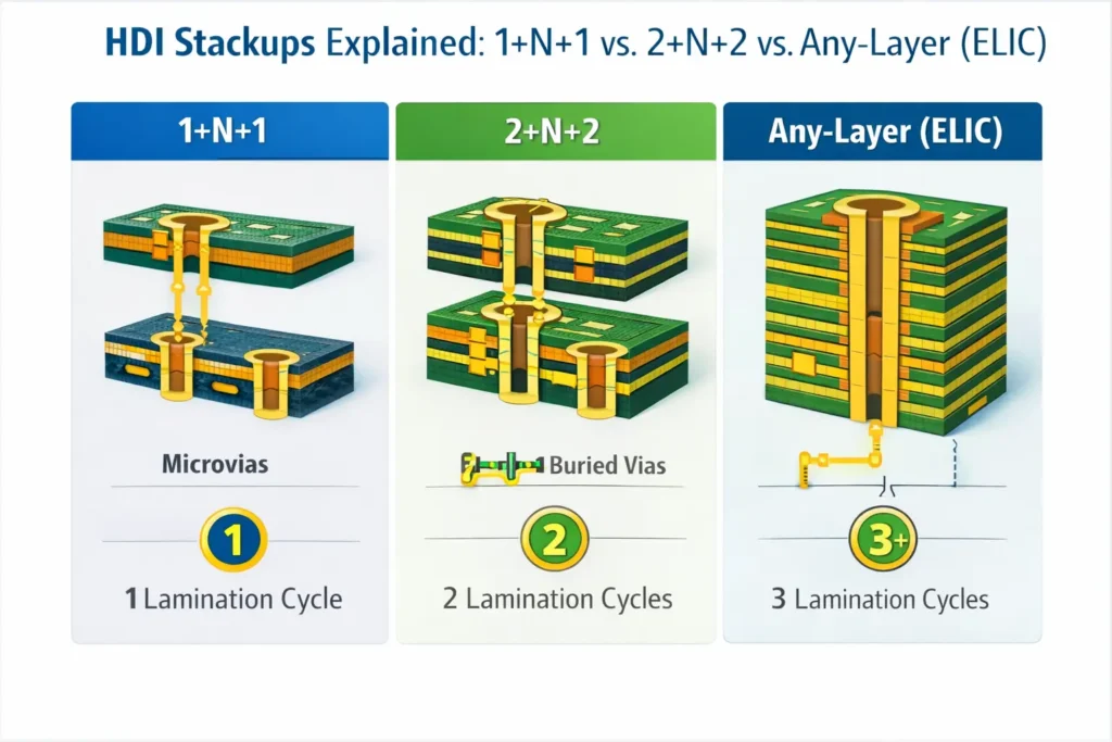
Understanding the notation: 1+N+1, 2+N+2
N = the core layer count (traditional multilayer core)
“+1” = a build-up (HDI) layer added via sequential lamination on one side
Type I (1+N+1): the entry point
One HDI build-up layer on each side of a core
Common for moderate density BGA fanout and compact products
Usually the best cost/performance balance when it works
Type II (2+N+2): higher density and routing flexibility
Two build-up layers on each side
More microvias, more lamination steps, higher registration requirements
Often used in dense mobile boards, modules, compact compute
Type III (multiple build-up / higher complexity)
More build-up layers and potentially more complex via strategies
Higher density, but cost/yield sensitivity increases sharply
Any-Layer / ELIC (Every Layer Interconnect)
ELIC (often called any-layer HDI) means every layer can be interconnected using microvias (typically in a stacked arrangement with filling/capping).
Why it matters: maximum routing freedom and shortest vertical interconnect paths
Tradeoff: highest manufacturing complexity; via filling quality and registration control become critical
Procurement reality: If your design can work with 1+N+1 or 2+N+2, it often delivers most of the benefit at far lower risk than any-layer.
Microvias, Blind/Buried Vias, and Via-in-Pad (VIPPO)
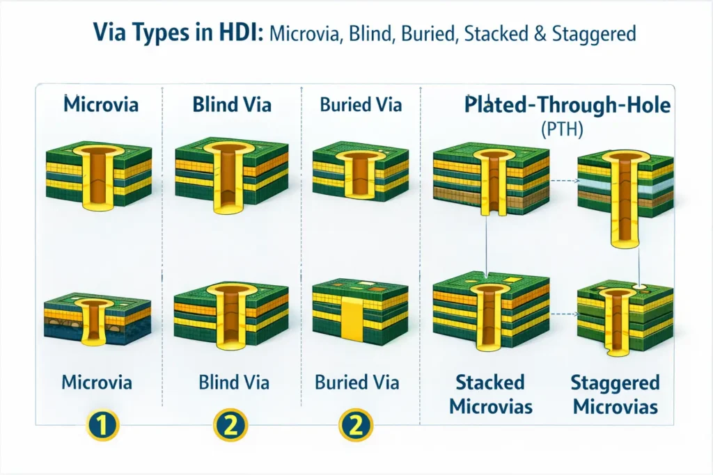
Microvias (laser vias)
Microvias are small vias typically formed by CO₂ or UV laser drilling. They are shallow and usually connect adjacent layers in build-up structures.
Key design rule (highly practical):
Keep microvia aspect ratio near ≤ 1:1 (depth ≤ diameter) for reliable plating/filling.
Blind vs. buried vias
Blind vias: connect an outer layer to one or more inner layers without going through the whole board
Buried vias: exist only between inner layers and never reach the surface
These structures:
reduce routing blockages
shorten via stubs
enable higher density without increasing board size
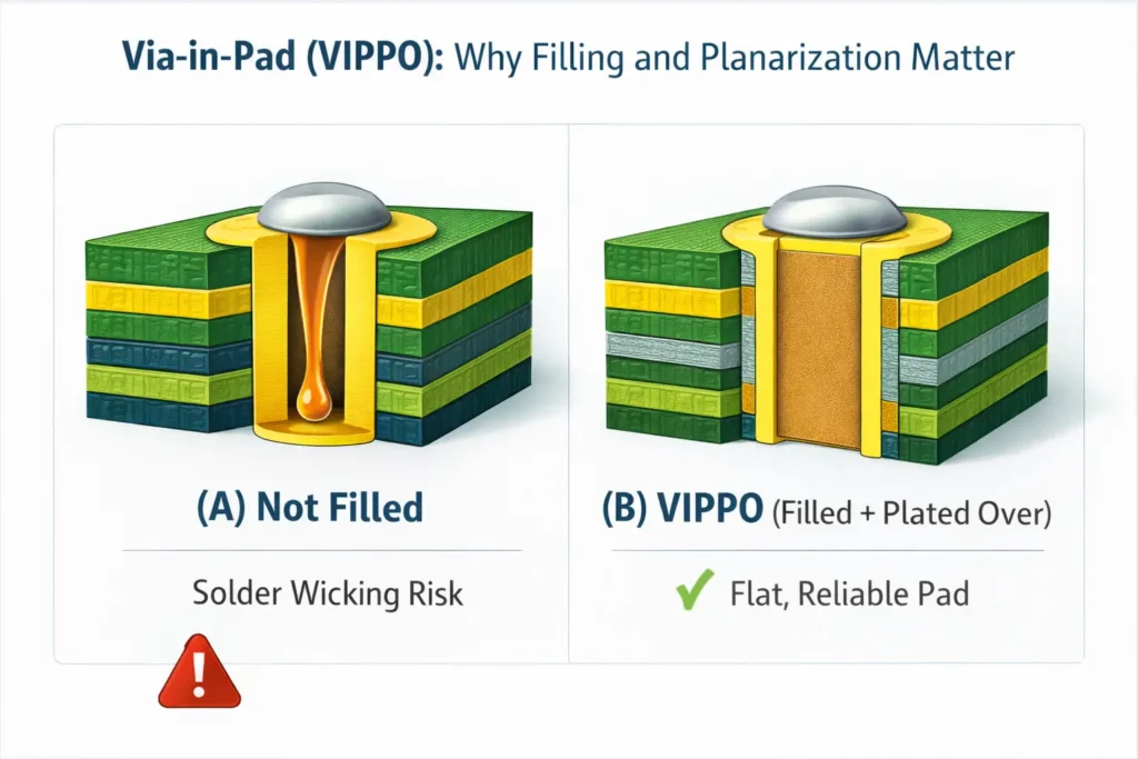
Via-in-pad and VIPPO (Via-in-Pad Plated Over)
For tight BGA pitches, you often need via-in-pad. But it must be done correctly:
VIPPO fills the via (copper or resin fill) and plates over it to create a flat pad surface
Prevents solder wicking into vias during reflow
Improves assembly yield in fine-pitch packages
Adds cost and process requirements (filling quality + planarization)
Why Choose HDI: Signal Integrity, EMI, and Space Optimization
Signal Integrity & high-speed design
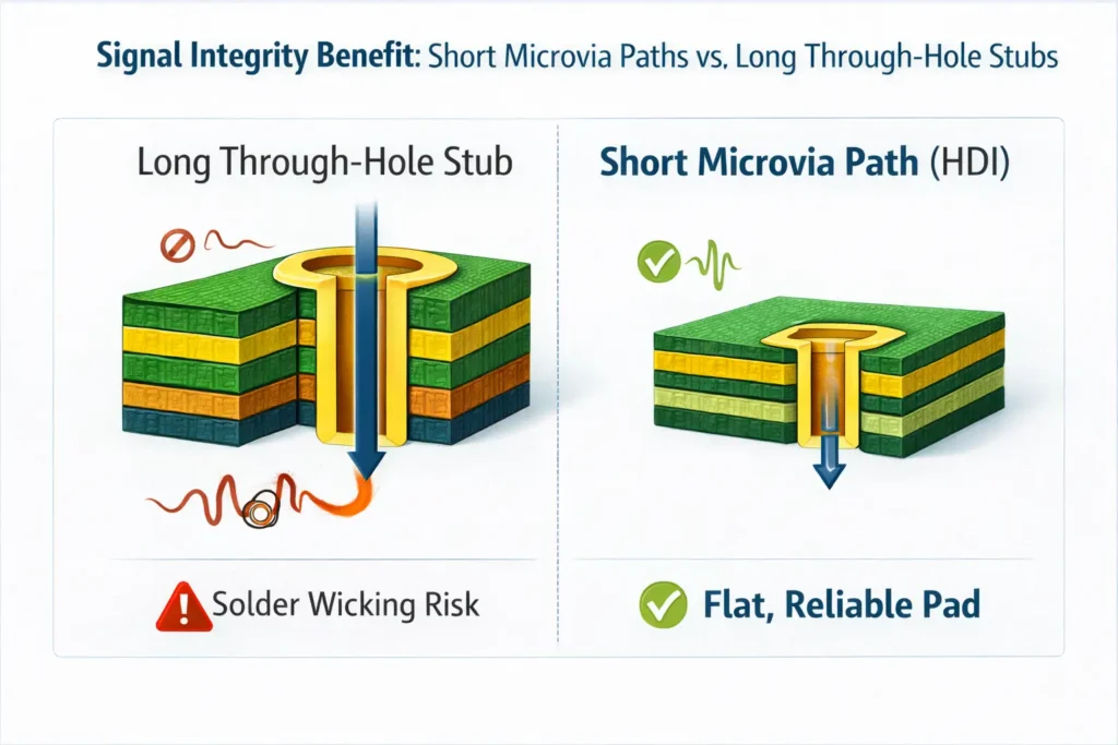
HDI helps high-speed design mainly by reducing parasitics and improving return path control:
Shorter vertical interconnects reduce parasitic inductance/capacitance
Reduced via stubs improves high-frequency behavior and lowers reflections
Fine routing + flexible stackups allow more consistent impedance control
Better layer planning allows cleaner return paths and reduced EMI risk
Where this matters most:
5G RF + high-speed digital combos
Smartphone SoCs and dense memory routing
Medical imaging and high-reliability sensing
Compact compute modules with tight SI budgets
Space optimization (how HDI reduces size or layer count)
HDI can reduce board size by:
enabling fanout in a smaller keep-out area
allowing signals to escape fine-pitch BGAs without “route jams”
freeing inner-layer channels that would be blocked by PTH vias
Important nuance: HDI does not always reduce layer count. Often it reduces board area, and sometimes it can reduce layers depending on routing congestion and constraints.
Materials for HDI: High-Tg, Low-Loss, RCC, and Copper Foils
Material choice affects loss, thermal reliability, and process stability.
Common HDI material needs
High-Tg resin systems: better thermal endurance (lead-free assembly, higher operating temps)
Low-loss laminates (low Dk/Df): reduce insertion loss and dispersion for high-speed signals
Halogen-free options: environmental compliance requirements
RCC (resin-coated copper) or build-up-friendly dielectric systems: often used to improve laser drilling behavior and fine-line imaging
Engineer + sourcing tip: Decide early whether only a portion of the stack needs low-loss materials (selective use can reduce cost).
HDI Manufacturing Process: Laser Drilling to Sequential Lamination
Key process steps (high-level)
Inner layer fabrication (etching inner circuitry)
Core lamination (forming the initial multilayer core)
Build-up dielectric + copper lamination (adding the next HDI layer)
Laser drilling microvias
Desmear + electroless copper (prepares via walls for plating)
Copper plating / via fill (as needed for stacked microvias / VIPPO)
LDI imaging (high-precision pattern transfer for fine lines)
Repeat steps 3–7 for each build-up cycle
Final finish + solder mask + surface finish + electrical test
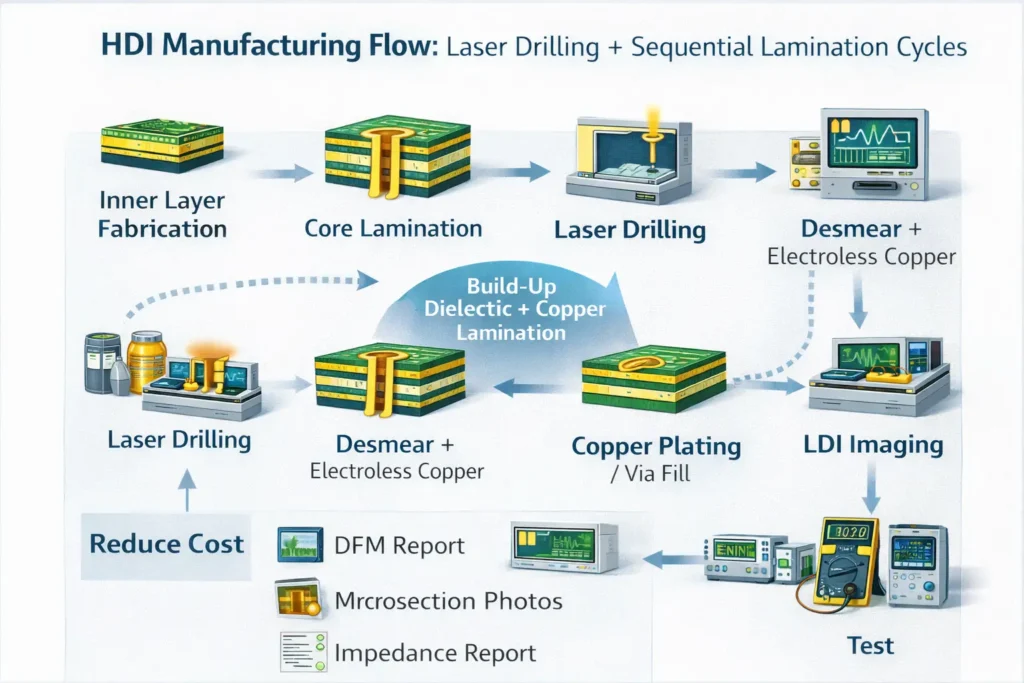
Why LDI matters in HDI
As line/space shrinks and registration tolerance tightens, LDI helps maintain pattern fidelity and alignment, improving yield.
Quality Control for HDI: What to Test and What to Request
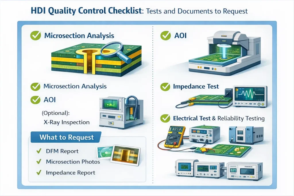
HDI quality cannot be validated by appearance alone. Strong QC typically includes:
Microsection (cross-section) analysis
Confirms plating thickness, fill quality, voids, cracks, layer alignmentAOI for outer-layer fine-line defects (opens/shorts/nicks)
X-ray for hidden structures (via fill quality, alignment checks in some workflows)
Impedance testing (especially for controlled impedance designs)
Reliability testing depending on application (thermal cycling, solder shock, etc.)
Procurement checklist: ask for these documents
DFM report (via strategy, annular ring, spacing, stackup feedback)
Microsection photos (representative, redacted if needed)
Impedance test report (if applicable)
Process capability statement (line/space, microvia, registration)
DFM and Cost Optimization: Avoiding Pitfalls and Cutting Cost Drivers
Common HDI design pitfalls (and what to do instead)
Overusing stacked microvias
Risk: higher stress concentration and stronger reliance on fill quality
Fix: use staggered microvias when routing allows
Mixed stacked + staggered strategy without planning
Risk: discontinuities, manufacturing complexity, unexpected yield loss
Fix: define a clear via architecture rule-set early
Via-in-pad without proper fill and planarization (VIPPO)
Risk: solder wicking → opens/weak joints
Fix: specify VIPPO requirements clearly (fill type, flatness criteria)
Ignoring lamination shrink/registration realities
Risk: pad misalignment, breakout, opens
Fix: lock stackup early and request CAM/DFM compensation guidance
Pushing line/space “too close to the cliff”
Risk: lower yield and increased cost from tighter process windows
Fix: use tiered rules—only push extremes in the smallest critical zones
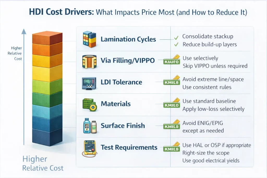
How to reduce HDI cost (high-impact levers)
Reduce lamination cycles: the biggest cost driver in many HDI builds
Minimize via filling: use it only where necessary (e.g., VIPPO, stacked microvias)
Avoid over-tight design rules unless required
Standardize materials where possible (availability and process maturity matter)
Panelization-friendly board outline: improves utilization and reduces unit cost
Early DFM review: prevents expensive redesign and tooling churn
Solving Common HDI Challenges: Thermal and Crosstalk
Thermal management in high-density boards
Use thermal via arrays under hot components to spread heat into internal planes
Increase copper area and thickness strategically (power planes, heat spreaders)
Consider higher-Tg materials for thermal cycling durability
If power density is high, plan mechanical cooling interfaces early (heatsink contact, airflow)
Signal interference and crosstalk solutions
Keep clean reference planes adjacent to critical signal layers
Maintain consistent impedance and avoid unnecessary layer transitions
Use spacing rules (e.g., avoid long parallel runs) and consider guard traces where appropriate
Differential pairs: enforce coupling and length matching where required
Validate critical nets with SI/PI simulation when budgets are tight
Finding a Reliable HDI PCB Manufacturer in China
China—especially Shenzhen and the Pearl River Delta—has dense supply chains and strong HDI manufacturing capacity. The key is selecting the right capability match.
Equipment matters (what to look for)
Laser drilling capability suitable for your microvia tier
LDI for fine-line imaging and registration control
Via filling / planarization capability if you need VIPPO or stacked microvias
AOI + reliable electrical testing
Cross-section lab (microsection verification)
Engineering support matters even more
The best HDI suppliers provide:
fast DFM feedback (stackup, via architecture, impedance planning)
manufacturability suggestions that reduce cost without sacrificing reliability
clear documentation and responsiveness during prototype-to-mass transitions
Future Trends of HDI
HDI continues to evolve toward:
finer line/space (including mSAP-style processes)
more integration with advanced packaging concepts
broader adoption in AI, automotive electronics, AR/VR, and high-speed interconnect products
Ready to start your HDI project? Upload your Gerber files to request a DFM review and quote. A fast DFM loop is the best way to confirm stackup feasibility, via strategy, and cost drivers before you commit.
FAQ
Is HDI more expensive than standard FR-4 PCB?
Often yes at the board level, because sequential lamination and microvia processes add cost. However, HDI can reduce total system cost by shrinking board size, improving performance margin, and enabling integration.
When should I choose 1+N+1 instead of 2+N+2?
If your BGA pitch and routing congestion can be satisfied with one build-up layer per side, 1+N+1 usually offers the best cost/yield balance.
Are stacked microvias reliable?
They can be reliable when fill quality, plating, and registration are tightly controlled. If you don’t need stacked microvias, staggered options often reduce risk and cost.
Do I always need via-in-pad (VIPPO) for fine-pitch BGAs?
Not always. If dogbone fanout is feasible, it may be lower cost. For very tight pitch and dense escape routing, VIPPO is often necessary.
What should I send for an HDI quote?
Gerbers, stackup requirements, impedance targets, via strategy (if known), IPC class needs, surface finish, quantity, and delivery schedule. If you’re unsure, ask for a DFM-first quote.

一个回复