Table of Contents
The Ultimate Guide to Multilayer PCBs: Design, Manufacturing, and Sourcing Strategies
Why Multilayer PCBs Define Modern Electronics
In the era of 5G, IoT, and high-performance computing, the demand for smaller, faster, and more powerful electronic devices has never been higher. Central to this transformation is the multilayer PCB. Unlike its simpler predecessors, multilayer boards enable higher component density and more complex circuitry within a compact footprint.
As a leading PCB and PCBA factory based in Shenzhen, with over 15 years of experience, we understand how a well-designed multilayer stack-up can make the difference between a high-performing product and a costly failure. Whether you are a hardware engineer optimizing signal integrity or a procurement manager searching for a reliable PCB manufacturing partner, this guide provides the technical and commercial insights you need.
Fundamentals: What is a Multilayer PCB?
Definition and Core Structure
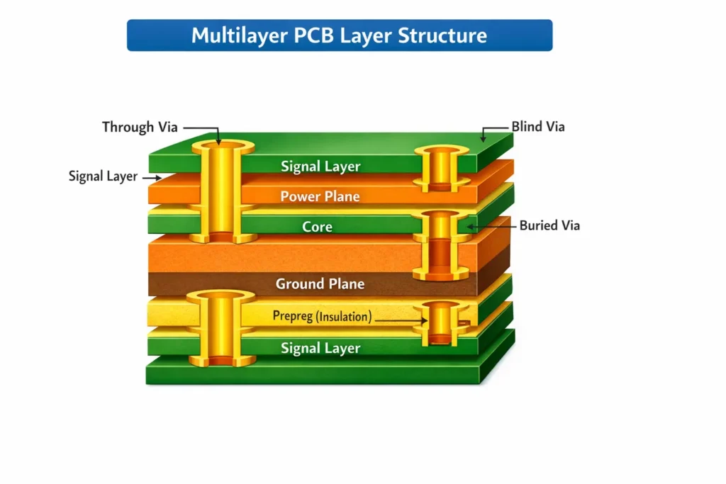
A multilayer PCB is a printed circuit board consisting of three or more conductive copper layers, which are separated by insulating materials such as Prepreg and Core. These layers are then bonded together under high temperature and pressure to form a single rigid board.
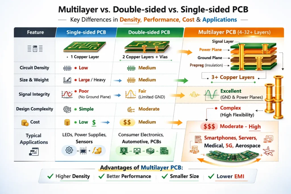
Multilayer vs. Single/Double-Sided PCBs
While single-sided PCBs are suitable for simple electronics such as LED lights and basic sensors, multilayer PCBs are crucial for complex electronics requiring higher performance and reliability.
| Feature | Single/Double-Sided | Multilayer PCB |
|---|---|---|
| Circuit Density | Low | High to Ultra-High |
| Size & Weight | Larger/Heavier | Compact/Lightweight |
| Signal Integrity | Limited | Excellent (due to ground planes) |
| Cost | Low | Moderate to High |
| Applications | LED lights, Simple sensors | Smartphones, Servers, Medical devices |
Anatomy of a Layer Stack-up
A typical multilayer board isn’t just a simple copper sandwich. It involves:
Signal Layers: Where electrical signals are transmitted.
Internal Planes (Power & Ground): These layers distribute power and provide a return path for signals, significantly reducing electromagnetic interference (EMI).
Engineering Deep Dive: How Multilayer PCBs Work
The Critical Role of Stack-up Design
The stack-up is the DNA of your PCB. A professional PCB manufacturer ensures symmetry in the stack-up to avoid warpage (bending) during the high-heat soldering process. Asymmetry in the design can lead to thermal stress, which can distort the board.
Signal Integrity & Controlled Impedance
For high-speed applications (such as DDR4 or HDMI), controlled impedance is critical. By precisely calculating the distance between the signal layer and reference ground plane, we ensure that signals travel without distortion or loss.
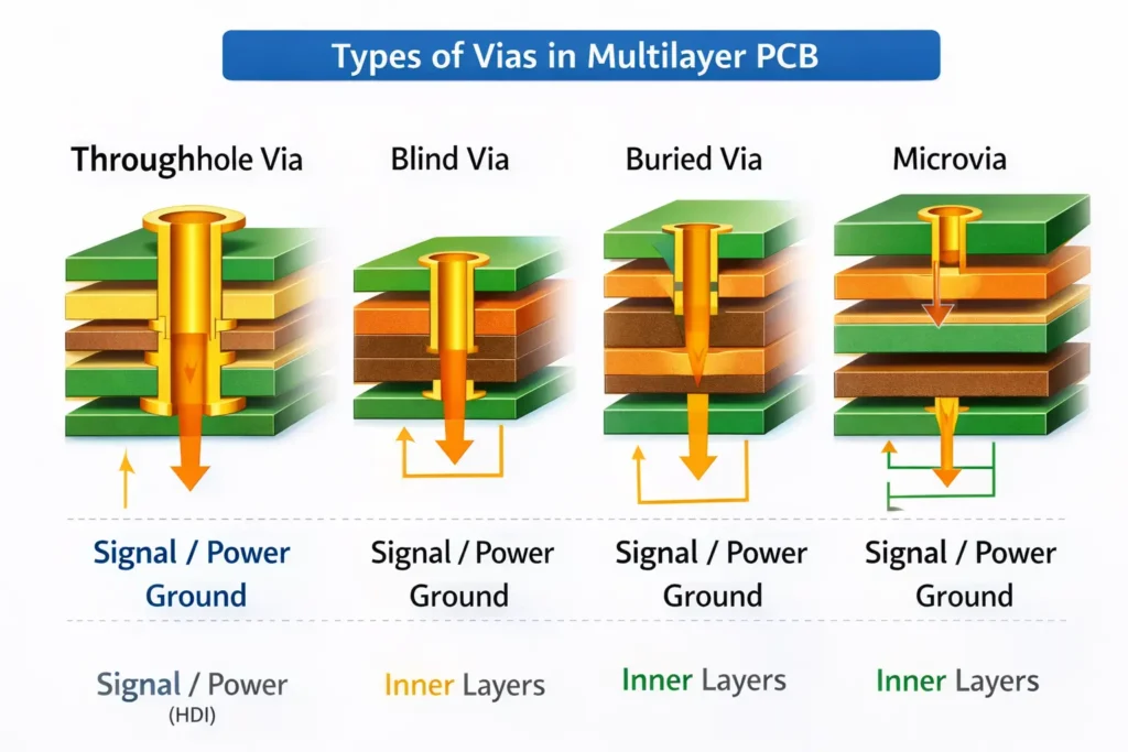
Interconnection via Vias
To connect different layers, we use various types of vias:
Through-hole Vias: Connect the top to the bottom layer.
Blind Vias: Connect an outer layer to one or more inner layers.
Buried Vias: Only connect internal layers without reaching the outer layers.
Microvias: Small holes (usually laser-drilled) used in HDI (High-Density Interconnect) designs.
Key Benefits: Why Upgrade to Multilayer Design?
Space-Saving and Lightweight
By stacking layers vertically, you can reduce the overall PCB size by 50% or more, making it ideal for applications like wearable devices and aerospace where size and weight are critical.
Enhanced Electrical Performance
Internal ground planes shield signal layers from external noise, resulting in superior EMI and EMC performance.
Increased Durability
The lamination process creates a robust structure that is more resistant to mechanical stress than traditional single-layer or double-layer boards.
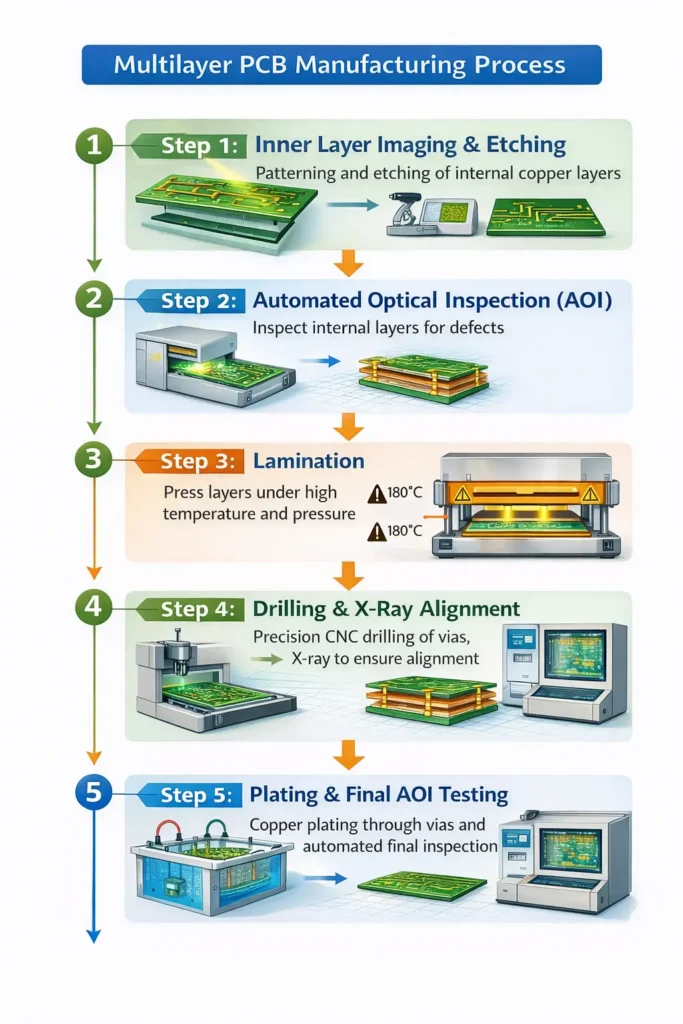
Manufacturing Process: From Design to Finished Board
At our Shenzhen facility, we use precision manufacturing steps to produce multilayer PCBs that meet the highest standards of quality:
Inner Layer Imaging: We start by etching the internal copper layers.
AOI (Automated Optical Inspection): A critical step to inspect each internal layer for defects before lamination.
Lamination: Layers are stacked with Prepreg and bonded under vacuum pressure at high temperatures.
Drilling & X-Ray Inspection: X-ray machines ensure micron-level accuracy in drilling.
Plating & Outer Layering: Electroplating is used to form vertical interconnects (vias).
Design for Manufacturing (DFM) & Cost Optimization
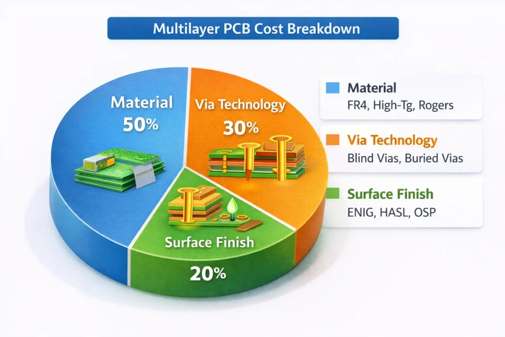
Factors Influencing Multilayer PCB Cost
Layer Count: More layers increase cost due to additional materials and complex processes.
Via Technology: Blind and buried vias require additional drilling and lamination cycles, increasing the price.
Surface Finish: ENIG (Electroless Nickel Immersion Gold) provides flatness but is more expensive than HASL (Hot Air Solder Leveling).
How to Reduce Costs Without Sacrificing Quality
Standardize Layer Thickness: A 1.6mm thickness can reduce costs without affecting performance.
Avoid Over-Specification: Don’t over-engineer trace widths if they don’t significantly impact your design.
Consult Early: A DFM review before finalizing your design can save significant costs in production.
Industry Applications: Where Multilayer PCBs are Essential
Telecommunications: 5G base stations and network switches require complex multilayer boards.
Medical Electronics: MRI machines and ultrasound devices rely on high-reliability multilayer circuits.
Automotive: With EVs and ADAS (Advanced Driver Assistance Systems), automotive PCBs need multilayer designs that meet IATF 16949 standards.
Sourcing Strategy: Choosing the Right Partner in Shenzhen
When sourcing from China, not all factories are equal. For multilayer projects, evaluate your partner on:
Technical Capability: Can they handle 3mil/3mil line width/spacing?
Quality Standards: Do they support IPC Class 2 or Class 3?
Certifications: Look for ISO9001, UL, and IATF16949.
FAQ – Frequently Asked Questions about Multilayer PCBs
What is a multilayer PCB, and how does it differ from single-sided or double-sided PCBs?
A multilayer PCB is a printed circuit board that contains three or more conductive copper layers, separated by insulating materials like Prepreg and Core. This allows for higher component density, complex circuit designs, and improved signal integrity. Unlike single-sided or double-sided PCBs, which are limited in space and functionality, multilayer PCBs provide the versatility needed for high-performance applications such as smartphones, servers, and medical devices.
How many layers can a multilayer PCB realistically have?
Multilayer PCBs can have between 4 to 32 layers, with some advanced applications reaching 60+ layers. For most consumer electronics, 4 to 8 layers are typical, while more complex aerospace or telecommunications designs might require up to 32 layers. Our factory can handle up to 32 layers comfortably, providing flexibility for a wide range of designs.
What are the key factors influencing the cost of a multilayer PCB?
The cost of a multilayer PCB depends on factors like layer count, via technology, and material choice. The more layers you add, the higher the cost due to the increased complexity in manufacturing. Special materials like Rogers or high-Tg FR4 and advanced vias such as blind and buried vias further increase the cost. Surface finishes (e.g., ENIG vs. HASL) and DFM considerations also impact the overall price.
How does signal integrity improve in multilayer PCBs?
Signal integrity is enhanced in multilayer PCBs through the use of internal ground and power planes, which act as shielding layers. By placing signal layers between these planes, electromagnetic interference (EMI) is reduced, and signal loss is minimized. This is particularly important for high-speed applications like 5G, DDR4, and HDMI, where precise impedance control and low signal distortion are crucial.
Why should I source multilayer PCBs from Shenzhen, China?
Shenzhen is renowned as the global hub for PCB manufacturing, offering rapid prototyping and scalable production with a highly efficient supply chain. Our factory in Shenzhen provides competitive pricing, advanced manufacturing capabilities, and a high-quality production process. The proximity to electronics suppliers and shipping routes ensures fast turnaround times, making Shenzhen the ideal location for sourcing multilayer PCBs.
Conclusion
Multilayer PCBs are the backbone of modern innovation. Understanding the nuances of stack-up design, material selection, and manufacturing constraints is key to a successful product launch.
Planning a complex multilayer project?
Contact our Engineering Team for a free DFM check and a competitive quote.