Table of Contents
What Is Printed Circuit Board ?
Overview

What is PCB ?
A PCB (Printed Circuit Board) is the physical foundation of an electronic device. It serves as both the mechanical support for electronic components and the electrical interconnection platform that enables the circuit to function. A PCB is built from an insulating substrate and the conductive structures attached to it—such as copper traces, pads, and vias. By using a pre-designed circuit pattern instead of traditional manual wiring, PCBs enable precise, reliable, and repeatable electrical connections between components.
You can think of a PCB as the “nervous system” of an electronic product: it allows different functional modules to communicate, ensuring the device operates stably and consistently.
Why Are PCBs Essential in Modern Electronics?
Miniaturization and high integration
Multilayer structures and fine-pitch routing allow complex circuits to be implemented within limited space, supporting compact and high-performance products.Reliability and consistency
Standardized manufacturing processes ensure repeatable electrical performance and reduce human error compared with manual wiring.More than electrical connections
PCBs play a critical role in power distribution, signal integrity, thermal management, and electromagnetic interference (EMI) control, directly affecting product stability and service life.
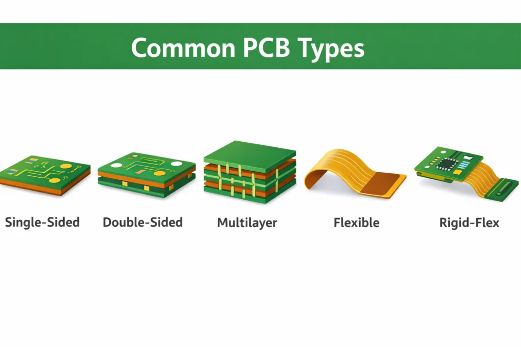
Different Types of PCBs
| PCB Type | Structural Features | Typical Applications | Advantages | Limitations | Cost Level |
|---|---|---|---|---|---|
| Single-sided PCB | One copper layer | Simple circuits, basic consumer electronics | Lowest cost, simple process | Limited routing capability | Low |
| Double-sided PCB | Copper on both sides, through-holes | Industrial control, home appliances, automotive sub-modules | Higher routing density | Increased complexity and cost | Low–Medium |
| Multilayer PCB | 3 or more copper layers (usually even) | Communication systems, computing, complex control | High density, better signal integrity | Layer alignment and higher cost | Medium–High |
| Flexible PCB (FPC) | Polyimide or other flexible substrate | Wearables, camera modules, compact assemblies | Bendable, lightweight | Higher material and process requirements | High |
| Rigid-Flex PCB | Integrated rigid and flexible layers | High-end compact devices | Fewer connectors, higher reliability | Complex design and manufacturing | Very High |
Single-Sided PCBs
Components are mounted on one side, while traces are formed on the other side. Single-sided boards are structurally simple and typically the lowest-cost option, but routing area is limited—making them suitable only for very basic consumer electronics or simple circuits.
Double-Sided PCBs
Double-sided PCBs have conductive copper on both sides of the board. Electrical connection between the two sides is achieved through vias (plated through holes), enabling higher component density and more complex routing than single-sided boards. This is one of the most widely used PCB types.
Multi-Layer PCBs
Multilayer PCBs consist of three or more conductive layers separated by insulating dielectric layers, interconnected by vias. They enable higher component density, smaller product size, and improved reliability. In practice, multilayer stackups are often designed with an even number of layers.
Flexible PCBs
Flexible PCBs use flexible materials such as polyimide (PI). Their key advantage is that they can be bent or folded, allowing them to fit into compact installation spaces or applications requiring flexing for mechanical durability.
Rigid-Flex PCBs
Rigid-flex PCBs integrate rigid and flexible sections through lamination. Rigid sections support component mounting, while flexible sections provide interconnection. This design is widely used in premium compact devices and improves long-term reliability by reducing connectors and assembly steps.
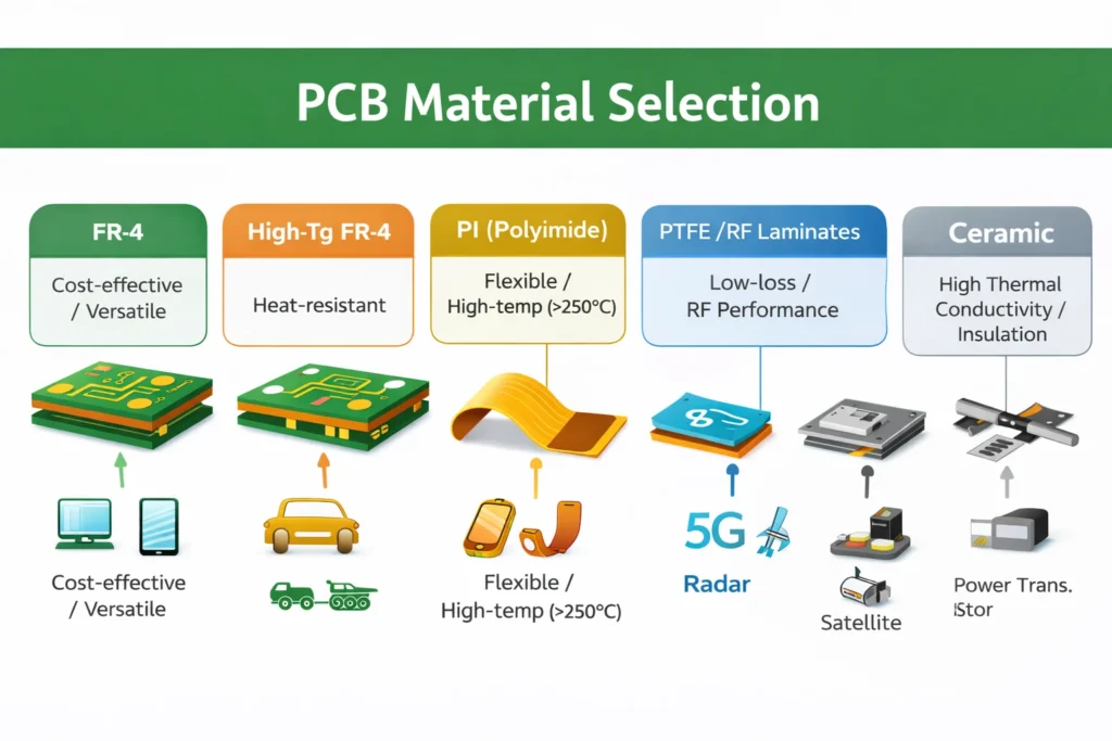
Materials used in PCB manufacturing
| Material | Core Characteristics | Typical Use Cases | Cost |
|---|---|---|---|
| FR-4 | Strong overall performance and high cost-effectiveness | General consumer electronics / industrial control | Low |
| High-Tg FR-4 | Improved heat resistance | Automotive, multilayer boards with multiple reflow cycles | Medium |
| Polyimide (PI) | >250°C heat resistance, flexible | FPC, high-temp environments, wearables | High |
| PTFE / High-frequency materials | Low loss, suitable for RF | 5G, radar, satellite | Very High |
| Ceramic-filled materials | Stable high-frequency performance, low CTE | High-frequency/high-speed modules | High |
| Aluminum/Copper core (MCPCB) | Excellent heat dissipation | High-power LEDs, power modules | Medium–High |
| Ceramic substrate | Ultra-high thermal conductivity + insulation, high-temp | Power semiconductors, aerospace, RF power modules | Very High |
Common PCB materials
Rigid PCB Materials
FR-4: The most widely used rigid PCB substrate. It is a composite of epoxy resin and fiberglass cloth and offers flame retardancy (commonly UL94-V0), good mechanical strength, and excellent cost-performance. It is widely used in consumer electronics, computing, and industrial control.
High-Tg FR-4: Uses high-temperature epoxy resin with a glass transition temperature (Tg) typically above 170°C, offering better thermal resistance for automotive electronics, defense applications, and other high-temperature environments.
Composite substrates (CEM series): Such as CEM-1 (paper fiber + epoxy resin, commonly used for single-sided boards) and CEM-3 (fiberglass + epoxy resin, performance close to FR-4, often used for double-sided boards).
Flexible PCB Materials
Polyimide (PI): The most common substrate for flexible circuits, offering excellent heat resistance (often above 250°C) and flexibility. Commonly used in smartphone FPCs, camera modules, and wearables.
Polyester (PET): Lower cost but lower performance (especially heat resistance). Typically used in less demanding flexible circuits such as keyboard membrane circuits.
High-Frequency / High-Speed Materials
For 5G communications, radar, and high-speed servers where signal integrity requirements are strict, low dielectric constant and low loss factor materials are commonly used:
PTFE-based materials: For example, the Rogers RO4000 series—very low dielectric loss and suitable for high-frequency applications.
Ceramic-filled materials: Ceramic powder combined with PTFE or epoxy resin systems (e.g., Rogers RO3000 series), offering stable high-frequency performance.
PPO (Polyphenylene oxide): Low dielectric constant, suitable for high-speed digital circuits such as server motherboards.
Metal core substrates (MCPCB)
Used when strong thermal performance is required:
Aluminum core: An aluminum plate + dielectric insulation layer (often epoxy-based) + copper foil. Strong heat dissipation; widely used in high-power LED lighting and power modules.
Copper core: Better thermal conductivity than aluminum core; used for high-power devices such as automotive power electronics.
How to Choose the Right Material for Your PCB Project
| Material Type | Core Characteristics | Typical Applications | Cost Level |
|---|---|---|---|
| FR-4 | Strong overall performance, high mechanical strength, flame retardant, excellent cost-performance | Computers, smartphones, appliances, general industrial control (most common) | Low |
| High-Tg FR-4 | Significantly better heat resistance than standard FR-4 | Automotive electronics, defense, multilayer boards (multiple reflow cycles) | Medium |
| Polyimide | High heat resistance (>250°C), excellent flexibility | FPC, smartphone interconnects, wearables, aerospace | High |
| PTFE | Ultra-low dielectric loss, excellent high-frequency performance | 5G base station antennas, mmWave radar, satellite communications, RF connectors | Very High |
| Ceramic-filled materials | Stable RF performance, low thermal expansion (CTE) | High-frequency/high-speed modules, power amplifiers | High |
| Aluminum/Copper core | Excellent heat dissipation | High-power LEDs, automotive power modules, motor drivers | Medium–High |
| Ceramic substrate | Ultra-high thermal conductivity and insulation, high-temp | Power semiconductors, aerospace electronics, RF power modules | Very High |
PCB manufacturing process
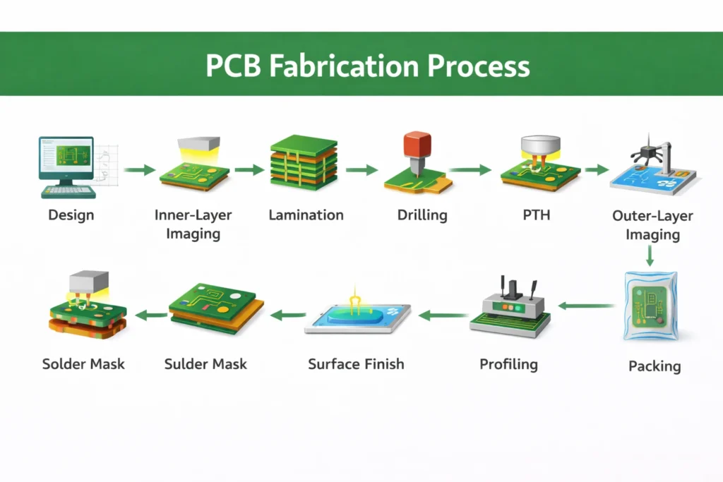
| Process Step | Key Actions | Common Risks | Typical Inspections |
|---|---|---|---|
| Inner-layer imaging | Exposure/development/etching | Opens, residual copper, line width deviation | AOI / inner-layer inspection |
| Lamination | Stack-up hot pressing | Misalignment, voids, delamination | X-ray / microsection (sampling) |
| Drilling | CNC / laser drilling | Hole offset, burrs | Hole inspection / dimensional measurement |
| Plated through hole (PTH) | Electroless copper + electroplating | Poor barrel plating | Microsection / electrical test |
| Outer-layer imaging | Plating build-up + etching | Shorts/opens | AOI |
| Solder mask / legend | Solder mask + silkscreen | Exposed copper, misregistration | Visual inspection |
| Surface finish | HASL / ENIG / OSP, etc. | Solderability variation | Solderability test / visual |
| Final electrical test | Flying probe / fixture | Escapes if coverage is poor | Electrical test coverage control |
PCB Design
PCB fabrication begins with design. Engineers create a circuit schematic and then use CAD tools to convert it into a PCB layout, defining component placement, routing, pad sizes, and the layer stack-up to meet electrical and mechanical requirements.
Imaging and Etching
Panel cutting and inner-layer fabrication: Large copper-clad laminates are cut to size. For multilayer boards, inner layers are fabricated first: after cleaning, a pattern transfer process (dry film lamination, exposure, development) forms the circuit image on copper. Protected copper remains after etching, while unwanted copper is removed using chemical etchants. Inner layers are then inspected and treated (e.g., oxide treatment) to prepare for lamination.
Lamination: Inner cores, prepregs (bonding material), and outer copper foils are stacked and laminated under heat and pressure—often in vacuum—to form a multilayer board.
Drilling: CNC drilling or laser drilling creates vias and component holes. For holes requiring interlayer electrical connection, metallization is performed.
PTH and outer-layer patterning: After drilling, hole walls are non-conductive. Electroless copper deposits a thin conductive layer, followed by electroplating to build copper thickness in holes and traces. Outer-layer pattern transfer is then performed, often using a “pattern plating” process: plating is applied where copper is needed, and unwanted copper is etched away.
Etching: For both inner and outer layers, after imaging, chemical etching removes copper in non-circuit areas, leaving clean trace patterns.
Solder Mask, Silkscreen, and Surface Finish
Solder mask: A permanent protective coating (typically green, but available in other colors) is applied to cover areas except pads that need soldering. It prevents shorts during assembly and protects copper from oxidation and scratches.
Silkscreen (legend): Component reference designators, polarity marks, and revision information are printed for easier assembly, debugging, and maintenance.
Surface finish: A protective layer is applied to exposed pads to prevent oxidation and ensure solderability. Common finishes include HASL, ENIG, immersion silver, and OSP. Depending on the process, this step may occur before or after solder mask.
Profiling, Assembly, and Testing
Profiling: The final board outline is formed via routing/milling, V-scoring for panelization, and other processes.
Component placement and soldering (assembly): This typically occurs after the bare PCB is manufactured, at an SMT assembly facility. Components are placed by pick-and-place machines and soldered via reflow, achieving electrical and mechanical connection. “Component placement” in many discussions refers to this assembly stage, not bare-board fabrication.
Testing and quality control: QC runs throughout production. Final testing commonly includes flying probe testing or dedicated fixtures to validate continuity and isolation, preventing shorts/opens. Additional methods such as AOI and X-ray may be used. After inspection, boards are vacuum packed for moisture and oxidation protection before shipment.
PCB Applications in Electronics
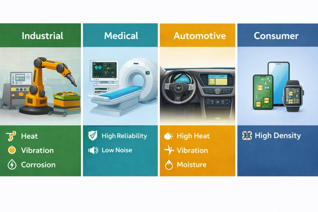
| Industry | Main Focus | Typical Requirements / Recommendations | Typical Tests / Standards Direction |
|---|---|---|---|
| Industrial control | Stability / anti-interference | Heat resistance, corrosion resistance, reliable interconnects | AOI + electrical test + reliability sampling |
| Medical electronics | High reliability / low noise | Strict consistency and traceability | More stringent QC systems (e.g., medical QMS) |
| Automotive electronics | Heat / vibration / moisture resistance | High-Tg materials, protective coatings | Reliability and environmental stress validation |
| Consumer electronics | High density / lightweight | HDI, multilayer, high-speed | SI/EMC design + assembly yield control |
Industrial control
Automation control: PCBs are widely used in robots, CNC machines, and automated production lines, acting as control modules that provide precise interconnects and control logic for stable operation.
High precision and system integration: Complex circuit design and high-precision fabrication enable fine control of equipment operation. PCBs also bridge subsystems, enabling efficient data transfer and system coordination.
Harsh environment adaptability: Industrial environments often involve heat, humidity, vibration, and corrosive exposure. Industrial PCBs require appropriate materials, mechanical strength, and stability to ensure reliable operation under harsh conditions.
Medical electronics
High reliability and precision: Devices such as ECG equipment, ultrasound systems, patient monitors, and CT systems rely on PCBs to acquire, process, and display signals. These applications require extremely high reliability and measurement accuracy.
Low noise and safety: Medical PCBs must minimize noise to avoid diagnostic interference and must comply with strict safety regulations.
Miniaturization and intelligence trends: Portable medical devices demand smaller PCBs and low-power designs, while advanced systems require high-performance, high-reliability PCBs to support precision treatment and intelligent management.
Automotive electronics
Environmental endurance and high reliability: Automotive PCBs must operate reliably in high temperatures (engine bay), vibration, humidity, and corrosive environments. Special materials and processes are commonly used to improve heat resistance, vibration resistance, and corrosion resistance.
Core applications in critical systems: PCBs are central to automotive electronics, including ECUs, infotainment, driver assistance systems, safety systems (ABS, airbags), and sensors.
Driven by intelligence and electrification: With ADAS and connected vehicles, automotive PCBs must support faster, more stable data transmission with higher integration and signal integrity. EV growth also raises requirements for power density, thermal performance, and EMC.
Consumer electronics
High integration and miniaturization: Smartphones, tablets, laptops, TVs, and game consoles are classic PCB applications. Limited internal space requires high integration, often making HDI standard.
Performance and functionality core: PCB design directly impacts product performance. Smartphone PCBs must optimize placement for processors, memory, and RF modules to ensure stable communication and efficient processing. Audio products require careful layout, differential routing, and grounding for high-fidelity sound.
Accelerating technology evolution: Consumer demand for thinner, faster, and more feature-rich devices drives PCB technologies toward higher density, more layers, and higher-speed transmission.
PCB Standards and Quality Assurance
IPC Standards
PCBs must comply with industry standards to ensure reliability and safety. IPC standards—such as IPC-2221 (design standard) and IPC-A-600 (acceptability standard)—provide guidance for PCB design, fabrication, and inspection. Compliance helps ensure consistent quality and reliability.
Certifications and Quality Testing
In addition to IPC standards, PCB manufacturers often maintain certifications such as ISO 9001 (quality management) and UL safety certification. These certifications help verify that manufacturing follows robust quality control systems and meets international performance and safety requirements.
How to Choose the Right PCB
Key Factors to Consider
Application needs: Different industries require different reliability and compliance levels. For example, medical devices typically require stricter quality control, while consumer electronics often prioritize cost-performance.
Design complexity: More complex designs may require multilayer PCBs or flexible PCB solutions.
Operating environment: Temperature, humidity, vibration, and corrosive exposure influence material selection and design features.
Cost: Budget constraints affect material selection, process choices, and manufacturability.
Custom vs. Standard PCB Solutions
For specialized applications, custom PCBs may be required. Custom PCBs are tailored to specific design and performance requirements, offering greater flexibility but typically at higher cost. Standard PCBs are produced at scale and are more cost-effective, but may not meet the requirements of specialized applications.
PCB Cost Considerations
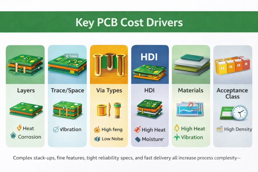
Key Cost Drivers
| Cost Driver | Why It Increases Cost | Typical Impact on a Project |
|---|---|---|
| More layers | More materials + more alignment/lamination steps + yield pressure | Costs often rise in a “stepwise” manner |
| Tighter trace/space | Higher precision and narrower process window | Higher scrap risk and inspection cost |
| Smaller/more holes | Longer drilling time + higher tool wear | Higher labor and complexity |
| Blind/buried vias / HDI | Additional processes (laser drilling, sequential lamination) | Significant cost increase |
| Upgraded materials | RF/ceramic/metal substrates cost more | Higher laminate cost |
| Advanced surface finishes | ENIG improves stability but costs more | Better for BGA / fine pitch |
| Higher acceptance class | Lower defect tolerance, more rework/scrap | Higher cost, lower risk |
Layer count
One of the most significant cost factors. As layer count increases, material usage rises and more processes are required (inner-layer fabrication, lamination, alignment), while yield pressure can increase. In general, costs often increase stepwise rather than linearly.
Board size and shape
Larger boards consume more material, increasing cost. Irregular shapes can increase processing complexity and material waste.
Design complexity and precision
Trace width/spacing: Smaller trace/space requires higher manufacturing precision and can increase scrap risk and cost.
Hole count and hole type: More holes increase drilling time. Smaller holes are more difficult and increase tool cost. Blind/buried vias require additional processes such as laser drilling and sequential lamination, significantly increasing cost.
Special process requirements: Controlled impedance, HDI, heavy copper (e.g., 2oz+), embedded resistors/capacitors, edge plating, gold fingers, etc., all add process steps and inspection requirements.
Laminate and copper thickness
Different laminates vary widely in price. Board thickness and copper weight (1oz, 2oz, 3oz) are also key cost variables—thicker copper increases material cost.
Surface finish
Different finishes have different cost and performance. ENIG is commonly chosen for BGA and high-density assembly due to excellent planarity and oxidation resistance, but it typically costs more than HASL.
Process standard and quality class
The acceptance level directly impacts yield and cost. For example, IPC-A-600 Class 3 has stricter acceptance criteria than Class 1, increasing manufacturing difficulty, scrap risk, and cost—while reducing field failure risk.
How to Get a PCB Quote
Contact PCBAgroup and share your Gerber/ODB++ files, layer count, board thickness, copper weight, material requirements, surface finish, impedance/HDI requirements, quantity, and lead time. Our engineers will provide DFM recommendations and a quotation, helping you balance cost, yield, and reliability.