Table of Contents
What Is PCB Electrical Testing
If you are sourcing printed circuit boards for a new product, one of the most important quality controls to ask about is PCB electrical test (often called E-test).
For engineers, electrical testing helps confirm that the fabricated board matches the design netlist before assembly.
For procurement teams, it reduces the risk of costly production delays, rework, and field failures caused by open circuits or shorts.
What Is PCB Electrical Test?
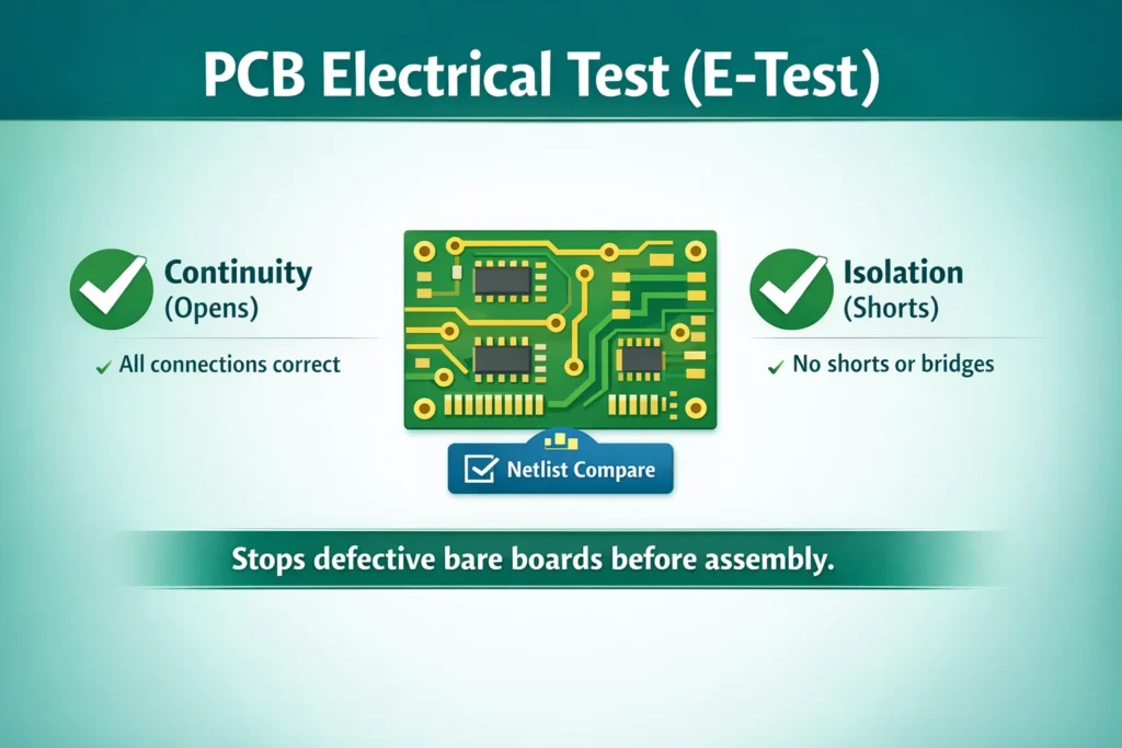
PCB electrical test is a verification process performed on a bare PCB (before components are assembled) to confirm the board’s electrical connectivity is correct.
In simple terms, the test checks whether:
All intended connections are connected (continuity)
No unintended connections exist (shorts / isolation failures)
The test result is typically compared against the PCB design data (netlist) to ensure the manufactured board matches the intended circuit connections.
Why PCB Electrical Testing Is Critical for Engineers and Manufacturers
Ensures functionality: confirms the design intent is realized
Connectivity tests verify, point-by-point, whether the designed nodes are properly connected, ensuring the circuit logic is correct and avoiding functional failure.
Protects reliability: blocks hidden failure risks
Insulation and parameter tests can identify latent defects (e.g., leakage, signal distortion), intercept reliability risks, and reduce after-sales costs.
Improves quality and efficiency: optimizes production and cost control
Real-time feedback helps detect process abnormalities and quickly adjust the line, enabling efficient automated inspection and meeting mandatory industry standards.
Supports iterative improvement: accelerates R&D
Analyzing failure modes provides engineers with data for design optimization and shortens the iteration cycle from design to verification.
PCB E-Test vs PCBA Testing
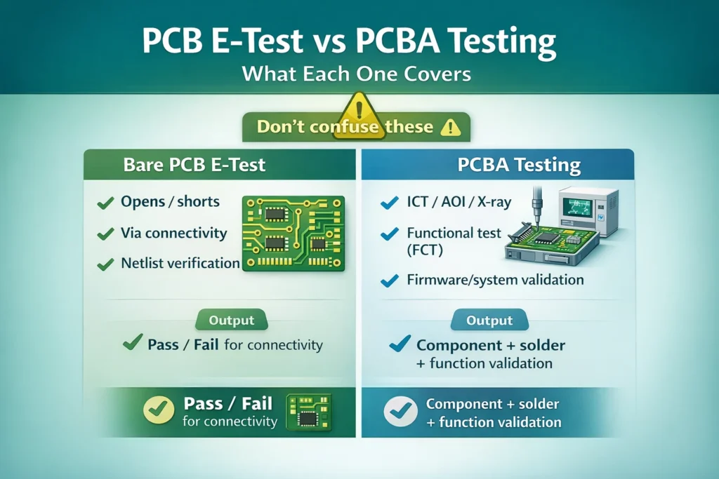
Bare PCB Electrical Test (E-Test) covers
Opens and shorts in copper networks
Via/through-hole connectivity issues
Netlist-based verification before assembly
PCBA tests (assembled boards) cover
Component presence/orientation and solder quality (e.g., ICT, AOI, X-ray/AXI)
Functional behavior under power (FCT)
Firmware/system-level validation
Practical takeaway: If your goal is to protect PCB fabrication quality before assembly, you want E-Test.
What E-Test Checks
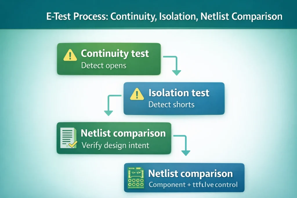
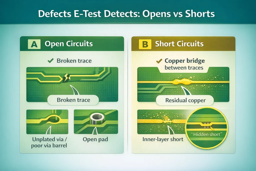
1) Continuity Test (Open-Circuit Detection)
This test verifies that points belonging to the same net are electrically connected.
Typical defects detected:
Broken traces
Incomplete plating in through-holes/vias
Open pads
Cracked copper connections
2) Isolation Test (Short-Circuit Detection)
This test verifies that different nets are electrically isolated from each other.
Typical defects detected:
Copper bridges
Residual copper causing shorts
Solder mask misalignment (if exposed copper causes risk)
Internal layer shorts in multilayer PCBs
3) Netlist Comparison
The manufacturer compares the measured connectivity against the required netlist generated from Gerber/CAM data (or customer-provided netlist, depending on process).
This ensures the board is tested against the intended design—not just against a visual inspection standard.
PCB Electrical Test Methods: Flying Probe vs Fixture Test
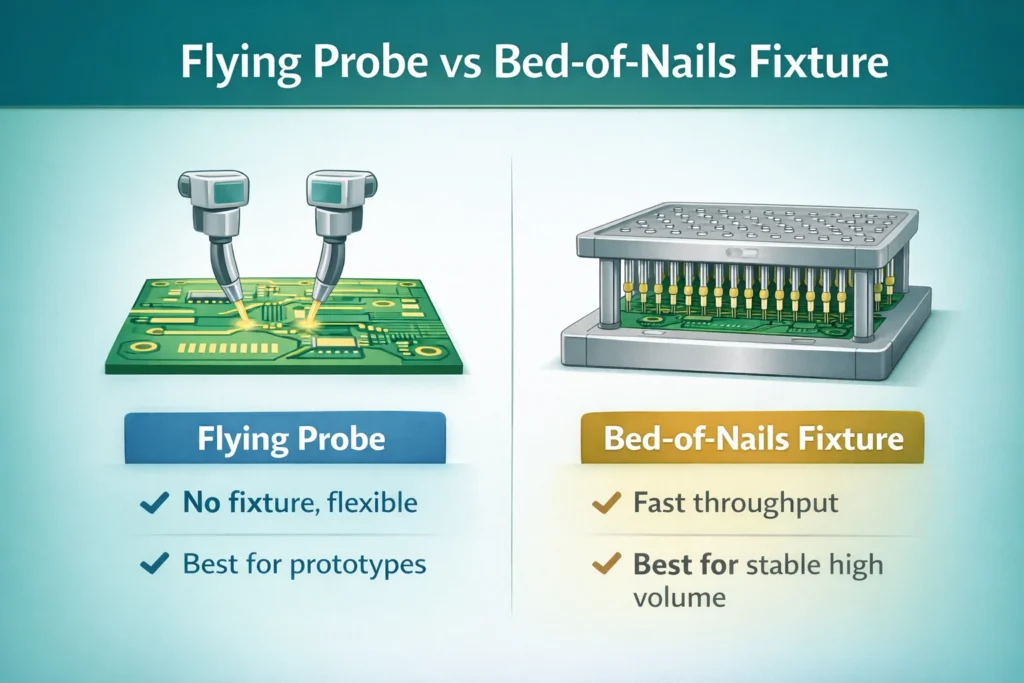
The choice between flying probe and fixture testing primarily depends on volume, design stability, cost structure, and lead time requirements.
| Item | Flying Probe Test (Fixtureless) | Fixture Test (Bed-of-Nails) |
|---|---|---|
| What it is | Software-controlled probes move to test pads/vias and measure continuity/isolation | A custom fixture with many spring-loaded pins contacts the board simultaneously |
| Best for | Prototypes (NPI), low–medium volume, high-mix, frequent design changes | Medium–high volume, stable designs, repeated orders |
| Upfront setup | No fixture required; programming/setup is relatively fast | Requires fixture design and build (upfront effort + time) |
| Unit test speed | Slower per board (probes move point-to-point) | Very fast per board (many points tested at once) |
| Cost behavior | Lower upfront cost; can be more expensive per board at high volume | Higher upfront fixture cost; lower per-board cost at volume |
| Flexibility | Very high—easy to adapt to multiple SKUs/ECOs | Lower—fixture updates needed for ECOs/design changes |
| Typical use stage | Prototype → pilot builds → low/mid production | Mass production for mature, stable products |
| Pros | No fixture cost, quick start, ideal for frequent revisions | High throughput, strong repeatability, efficient for production lines |
| Cons | Not as efficient for very large volumes | Fixture cost + lead time; less suitable for frequent design changes |
| When to choose (rule of thumb) | If you need speed to start, low risk for changing designs | If your design is stable and volume justifies the fixture |
What PCB Electrical Test Does Not Cover
PCB electrical test is essential, but it is not the same as:
PCBA in-circuit test (ICT)
Functional testing (FCT)
AOI (Automated Optical Inspection)
X-ray inspection
Burn-in or reliability validation
PCB E-Test vs PCBA Testing
PCB Electrical Test (Bare Board): checks copper connectivity (opens/shorts)
PCBA ICT / FCT: checks assembled board/components and functional behavior
This distinction matters because some buyers search “PCB electrical test” but are actually comparing all manufacturing test stages. A helpful article should clarify this early.
When Should PCB Electrical Test Be Performed?
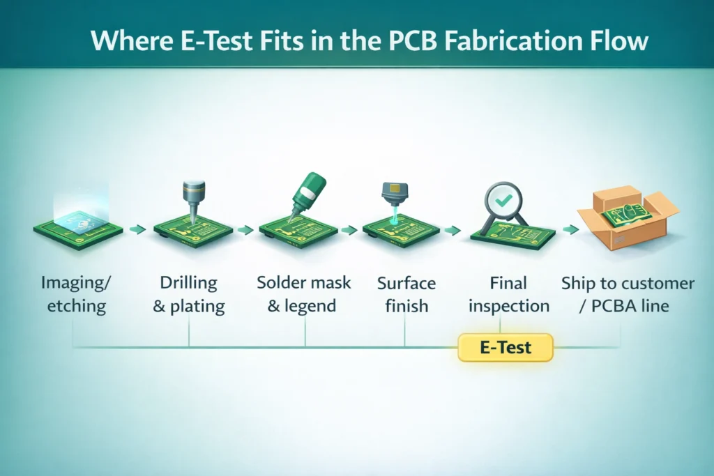
PCB electrical test is usually performed after fabrication is completed and before shipment.
1) PCB Fabrication Completed
Processes such as imaging, etching, drilling, plating, solder mask, legend, and surface finish are completed.
2) Final Inspection
Visual and dimensional inspections are performed (depending on process/requirements).
3) Electrical Test (E-Test)
The bare board is tested for opens/shorts against the netlist.
4) Shipment to Customer or PCBA Line
Only tested boards are released for shipment (depending on agreed quality plan).
For Prototypes
Electrical test is especially valuable in prototypes because it reduces debugging time caused by fabrication defects that can be mistaken for design errors.
For Mass Production
In volume production, it helps maintain consistency and reduce assembly-line yield loss.
What Affects E-Test Cost and Lead Time?
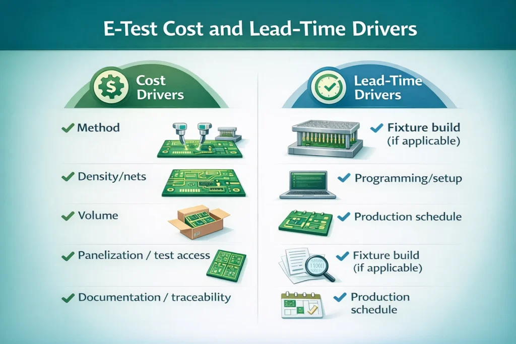
Cost Drivers
Test method (flying probe vs fixture)
Quantity and repeat frequency (one-time prototype vs recurring production)
Density/complexity (more nets, smaller spacing, HDI features)
Panelization and test point access
Any special requirements (documentation, traceability)
Lead-Time Drivers
Fixture build time (if fixture test is chosen)
Test programming/setup (especially for new designs)
Production schedule and throughput
Best practice: Decide your test strategy early (prototype vs production) so your supplier can quote accurately and avoid delays.
RFQ Checklist — What to Specify for PCB Electrical Test
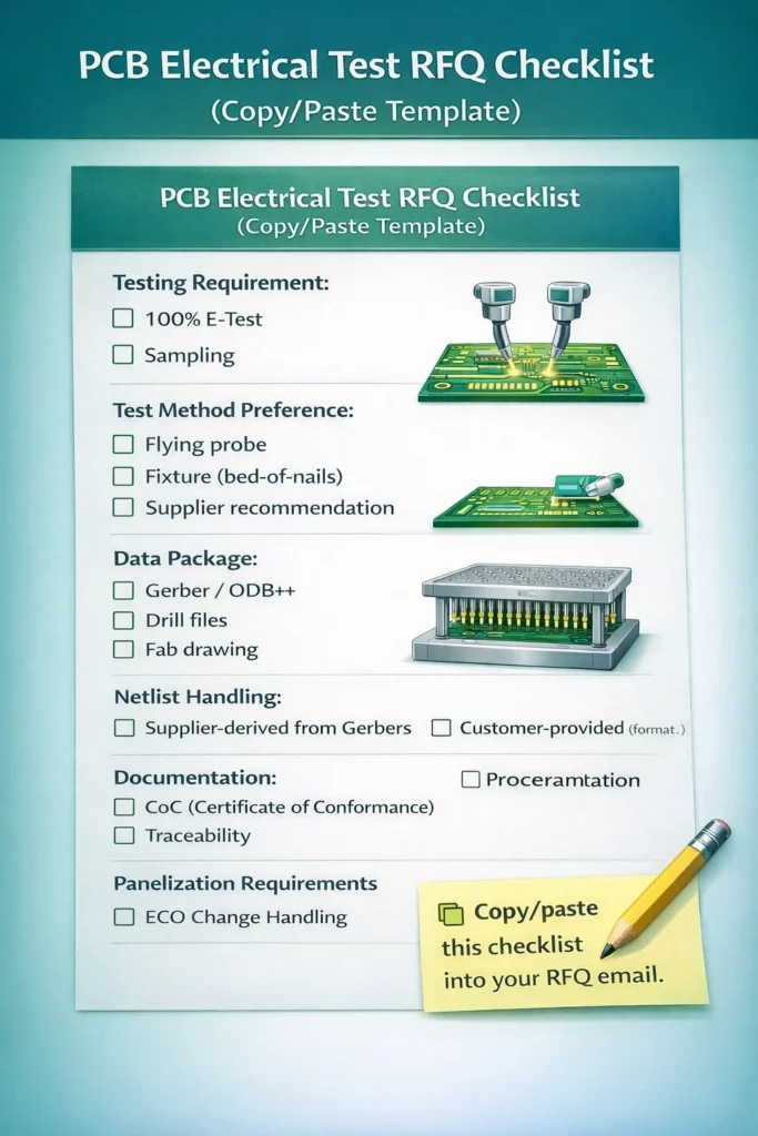
Testing Requirement
100% E-Test or sampling?
Test method preference: flying probe or fixture test (or “supplier recommendation”)
Data and Netlist
Confirm what data you will provide: Gerber/ODB++, drill files, fabrication drawing
Clarify netlist handling: customer-provided netlist (if applicable) or supplier-derived
Quality Documentation (if needed)
E-Test confirmation / CoC
Batch traceability requirements
Any special acceptance criteria (as agreed)
Practical Production Notes
Panelization expectations (if you require a specific panel format)
Design changes (ECO) handling: how retest/setup is managed
Best Practices
Provide Clean, Complete Manufacturing Data
Incomplete or inconsistent data increases CAM questions and can slow test programming. Provide:
Gerber or ODB++
Drill files
Stack-up notes (if controlled impedance is involved)
Fabrication drawing and special notes
Design for Testability (Bare Board Perspective)
If your design allows it, improve E-Test efficiency by:
Adding accessible test pads for key nets
Ensuring adequate probe clearance in dense areas
Avoiding unnecessary constraints that block test access
Treat “Signal Integrity / Reliability” as Related but Separate
E-Test validates opens/shorts and net connectivity.
If your project requires impedance validation, SI measurement, or environmental reliability testing, treat those as additional services with their own acceptance criteria and timelines.
FAQs About PCB Electrical Test
Is E-Test always 100%?
Not always—some programs use sampling based on risk, volume, or agreement. For many commercial and industrial products, buyers often prefer 100% E-Test to reduce downstream assembly risk.
Is flying probe enough for production?
For low-to-medium volumes or high-mix production, flying probe can be a practical solution. For stable high-volume programs, fixture testing often improves throughput and reduces per-board cost.
Does E-Test guarantee the final product will work?
No. E-Test verifies bare-board connectivity and isolation. Final product function depends on components, soldering, firmware, and system integration—covered by PCBA/functional testing.
What can I request from the PCB supplier?
Common requests include:
Confirmation of electrical testing performed
Test method description (flying probe vs fixture)
Traceability per batch (if required)
Conclusion
PCB Electrical Test (E-Test) is one of the most effective ways to prevent hidden fabrication defects from reaching assembly. It verifies opens/shorts and net integrity on bare boards, helping engineers reduce debugging time and helping procurement teams reduce production risk.
Send us your PCB files (Gerber/ODB++), quantity, layer count, and application notes. We can recommend the most suitable E-Test approach—flying probe for prototypes/high-mix or fixture testing for stable volume production—and provide an RFQ-ready quote.