Table of Contents
What Is PCBA? PCB Assembly Process, Cost, Testing & RFQ Checklist
Overview
What is PCBA ?
PCBA stands for Printed Circuit Board Assembly. It refers to a bare PCB that has gone through component placement, soldering, inspection, and often electrical testing, resulting in a board that can be powered and used as part of a product.
PCBA vs PCB: What’s the Difference ?
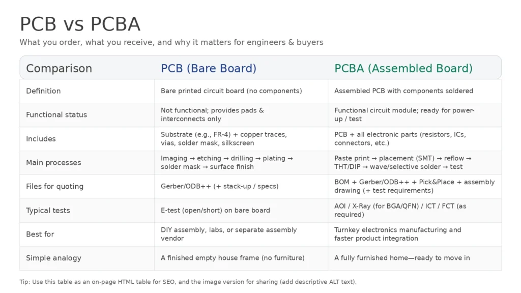
| Comparison | PCB (Printed Circuit Board / Bare Board) | PCBA (Printed Circuit Board Assembly / Assembled PCB) |
|---|---|---|
| Definition | A bare PCB made of insulating substrate (e.g., FR-4) with copper traces, pads, vias, solder mask, and silkscreen. It is the physical carrier and electrical interconnect foundation for electronic components. | A finished assembly after the bare PCB goes through SMT (surface-mount) and/or DIP/THT (through-hole) assembly processes. Components are placed and soldered to create a functional circuit module. |
| Functional Status | Not functional by itself; provides pads and routing only. | Functional (or ready for functional test); components are electrically connected and the board can be powered and tested. |
| Main Manufacturing Processes | Imaging → etching → drilling → plating → solder mask → surface finish (PCB fabrication steps). | Solder paste printing → component placement (SMT) → reflow → DIP/THT insertion → wave/selective soldering → cleaning (optional) → inspection & testing (AOI/X-Ray/ICT/FCT). |
| What’s Included | Board only: substrate + copper features + mask + silkscreen (no electronic components). | Board + all assembled components (ICs, resistors, capacitors, connectors, etc.)—a complete PCB + parts combination. |
| Simple Analogy | A house shell with wiring/plumbing routes—but no fixtures or furniture. | A fully finished home with furniture and appliances—ready to move in. |
 -->
-->
A PCB is the physical carrier for components and the electrical foundation (copper traces, pads, vias). A PCBA is the PCB plus all components assembled and soldered, forming a complete functional circuit module.
PCB = bare board (no parts)
PCBA = assembled board (components + soldering + inspections/testing)
Our Capability Snapshot


- Smallest components: 01005 (0.25 × 0.12 mm)
- Fine-pitch support: BGA pitch 0.3–1.0 mm; QFP pitch 0.3–1.0 mm
- Assembly lead time (assembly only): quick-turn options available (varies by quantity)
| Category | Capability | Notes |
|---|---|---|
| PCB size range | 50 × 50 × 0.5 mm to 510 × 460 × 4.0–4.2 mm | Max thickness may vary by board/process |
| Max board weight | Up to 2.0 kg | — |
| Materials | FR-4, CEM-1, CEM-3, Aluminium-based board, FPC | Material selection affects impedance/thermal behavior |
| Surface finish | HAL, OSP, Immersion Gold, Flash Gold, Gold Finger | Choose based on solderability & lifecycle |
| Smallest chip / IC | 01005 (0.25 × 0.12 mm) | High-density SMT supported |
| BGA pitch | 0.3–1.0 mm | X-Ray inspection recommended for hidden joints |
| QFP pitch | 0.3–1.0 mm | Fine-pitch alignment and AOI critical |
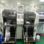
| SMT equipment (example) | Panasonic CM602 / NPM lines | Micro chip accuracy noted as ±35 μm (equipment spec) |
PCB size range: 50×50×0.5 mm up to 510×460×4.0/4.2 mm
Materials supported: FR-4, CEM-1, CEM-3, Aluminium-based board, FPC
Surface finish: HAL, OSP, Immersion gold, Flash Gold, Gold Finger
Smallest components: 01005 (0.25×0.12 mm)
Pitch capability: BGA pitch 0.3–1.0 mm; QFP pitch 0.3–1.0 mm
Placement performance (examples): 01005 at 50K CPH; BGA at 8K CPH; accuracy down to 0.03–0.04 mm (by type)
Typical assembly lead time (assembly time only):
SMD+connector: 5–200 pcs 6WD (quick 3WD)
SMD+DIP: 5–200 pcs 5WD (quick 4WD)
Note: lead time listed is for assembly time only
SMT lines / equipment mention: Panasonic CM602/NPM capability + micro chip accuracy ±35um and min size 01005
| Product type | Qty | Normal lead time | Quick-turn lead time |
|---|---|---|---|
| SMD + connector | 5–200 | 6 WD | 3 WD |
| SMD + connector | 201–2000 | 7 WD | 7 WD |
| SMD + connector | ≥ 2000 | 7–9 WD | 8 WD |
| SMD + DIP | 5–200 | 5 WD | 4 WD |
| SMD + DIP | 201–2000 | 7 WD | 5 WD |
| SMD + DIP | ≥ 2000 | 8 WD | 6 WD |
Note: Lead time above is for assembly time only. Component sourcing and PCB fabrication time depend on availability and specifications.
How PCBA Is Made
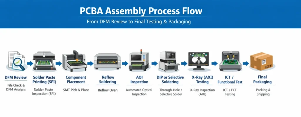
Input Stage: Engineering Review & DFM Check
1) Design file review
Manufacturers start by reviewing the package you provide: Gerber/ODB++, PCB design files, BOM, pick-and-place (centroid) data, assembly drawings, and test requirements. The engineering team verifies BOM completeness and accuracy—ensuring component values, packages, and part numbers match the design intent.
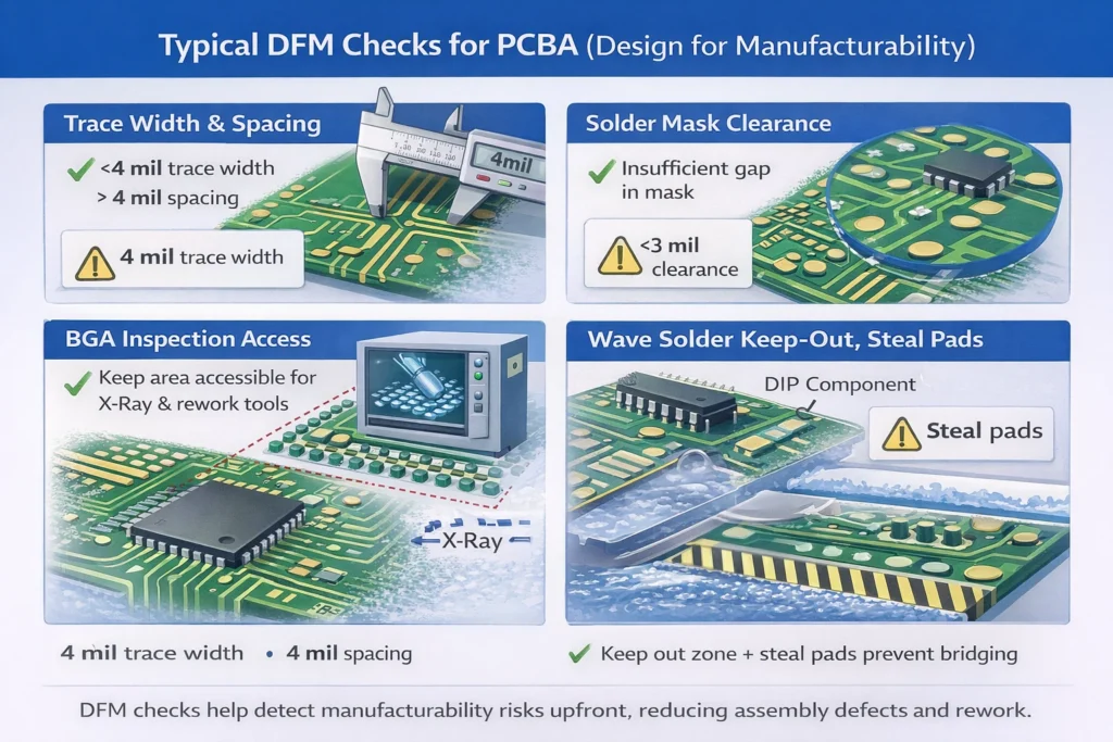
2) DFM (Design for Manufacturability) analysis
DFM is the core of the review. Engineers use professional tools and rulesets to evaluate whether the layout and footprints fit real production capability, including:
Trace/space, solder mask clearance, pad geometry
Component-to-component spacing and placement constraints
Thermal design considerations (heat spreading, hotspots, reflow sensitivity)
Manufacturability risks for complex packages such as BGA, including whether the design supports X-ray inspection and rework access
For boards requiring wave soldering, DFM rules are stricter. The solder-side needs adequate clearance around SMT parts (or fixture protection), and designers may add features like solder thieves to reduce bridging.
3) Risk prevention and action plan
DFM aims to identify risks early—such as solder bridging caused by tight spacing, or stress concentration caused by poor layout—and propose fixes before production. Close communication with the customer during this stage prevents avoidable delays and rework later.
SMT Process Overview
1) Solder paste printing & stencil setup
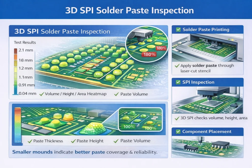
SMT begins with solder paste deposition. A custom laser-cut stencil is aligned to the PCB, and a squeegee prints solder paste through stencil apertures onto pads. Key controls include paste viscosity and particle size, plus printing pressure, speed, and alignment.
High-precision lines often perform 100% inspection using 3D SPI (Solder Paste Inspection) immediately after printing, monitoring paste volume/area/height in real time to prevent defects from flowing downstream.
2) Component placement
The paste-printed PCB enters a pick-and-place machine. Using the programmed centroid data, the machine picks components from reels, tubes, or trays and places them with micron-level accuracy (often in the tens of microns range) at the correct location and rotation.
Before placement, components typically pass IQC (Incoming Quality Control) to verify packaging integrity, labeling, condition, and sometimes electrical or authenticity checks.
Practical manufacturing note: pick-and-place lines have limited feeder slots, so reusing common components and reducing unnecessary part variety can improve efficiency and reduce changeover time.
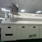
3) Reflow soldering
After placement, the PCB enters a reflow oven. A controlled temperature profile (preheat → soak → reflow → cooling) is tuned based on PCB materials, component heat tolerance, and solder paste chemistry to ensure reliable joints without thermal damage.
Advanced lines may use multi-zone reflow (e.g., 10–16 zones) with nitrogen protection, improving wetting and reducing oxidation—especially valuable for fine-pitch and high-density assemblies.
Through-Hole / DIP Assembly (Wave Solder vs Selective Solder)
1) Traditional wave soldering
The PCB passes over a continuous wave of molten solder, forming joints in one pass. Pros: high efficiency and low cost for high volume. Cons:
Larger thermal shock may affect already-mounted SMT components
Risk of bridging, insufficient solder, or shadowing
Often requires a custom wave solder pallet/fixture to protect SMT on the solder side, which adds cost
2) Selective soldering
A smaller solder nozzle solders only targeted through-hole joints by following programmed paths (point soldering or drag soldering). Key advantages:
Minimal heat exposure and small thermal influence area
Safer near dense SMT placement (mixed-technology boards)
Often reduces the need for complex pallets
Higher soldering quality and lower solder consumption
Trade-offs: equipment cost is higher, programming is more complex, and cycle time may be slower—yet it’s ideal for industrial, automotive, and high-reliability mixed-assembly boards.
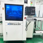
Inspection & Quality Control (AOI, X-Ray, Visual)
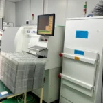
AOI (Automated Optical Inspection)
Post-reflow AOI scans the board with cameras and compares it against reference criteria to detect missing parts, wrong parts, misalignment, polarity errors, solder bridges, tombstoning, and other visible defects. AOI is fast, but cannot “see” under hidden joints.
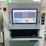
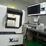
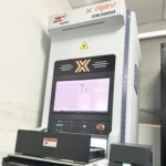
AXI / X-Ray inspection
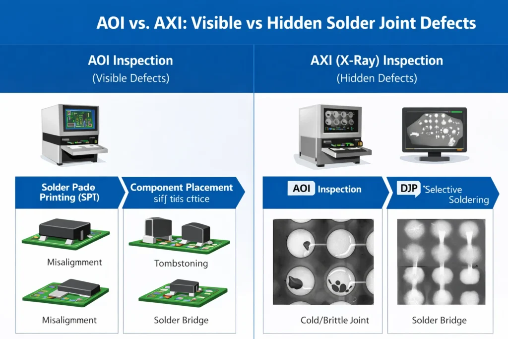
X-Ray inspection is essential for hidden-joint packages such as BGA, CSP, and QFN, detecting voiding, bridging, insufficient solder, and cold joints beneath components. Modern 3D AXI enables layered scanning and can also evaluate through-hole solder fill quality.
Visual inspection & IPQC
Manual checks complement automated tools, verifying edge cases and reducing false positives. IPQC (In-Process Quality Control) may also monitor key process parameters and perform sampling checks throughout production.
Functional Testing & Final Assembly
ICT and flying probe testing
ICT uses a bed-of-nails fixture to contact test points and quickly check opens/shorts and basic component values. It is fast and accurate but requires fixture investment. For prototypes or low volume, flying probe testing can reduce upfront cost without a dedicated fixture, at the expense of slower throughput.
FCT (Functional Circuit Test)
FCT powers the board and verifies system-level behavior under simulated or real operating conditions, checking I/O, communications, logic functions, and performance. This is often the final step that confirms the design meets functional requirements.
Firmware programming & burn-in
Programming can be done before assembly for some ICs, or after assembly via SWD/JTAG/UART or dedicated test interfaces. Burn-in testing may run boards under stress conditions (time, temperature, humidity, load) to screen early-life failures and improve shipment reliability.
Conformal coating & final assembly (optional)
For harsh environments (humidity, salt fog, corrosion risk), conformal coating is applied for protection. Some projects then proceed to final enclosure assembly as part of a box-build workflow.
Packaging, Labeling, and Shipping Considerations for Export Orders
ESD and moisture protection
PCBAs are ESD-sensitive. Standard packaging includes anti-static bags (often vacuum sealed or nitrogen filled), humidity indicator cards, and moisture control as required. Outer cartons should be strong, with shock-absorbing fillers to prevent impact damage during transit.
Labeling & traceability
Labels typically include model, revision, quantity, date code, lot number, and compliance marks (e.g., RoHS). Mature factories may assign each board a unique traceability code in an MES system, linking material lots, process steps, line/operator, and test data.
Documentation & compliance
Export shipments may include packing lists, commercial invoices, inspection/test reports (AOI/AXI/ICT/FCT), and compliance declarations (e.g., RoHS). For high-value shipments, choose appropriate transport (air vs sea) and purchase shipping insurance to reduce risk.
What You Need to Provide for a PCBA Quote
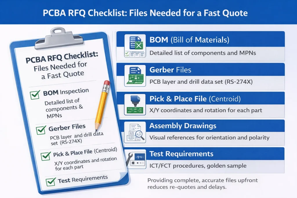
Must-Have Files (BOM, Gerbers, Pick & Place, Assembly Drawings)
BOM (Bill of Materials)
A quote-grade BOM should include: reference designators, description, package, electrical specs/value, brand, MPN, quantity, and clear notes on DNP parts. Avoid vague wording like “or equivalent” unless you define acceptable alternatives.
Gerber files
Gerbers are the blueprint for PCB fabrication. Provide complete layer sets including copper, solder mask, silkscreen, drill files, and board outline. Commonly used output format is RS-274X, with drill data (e.g., .drl). For blind/buried vias or special processes, clearly note requirements.
Pick-and-place (centroid) file
This file drives placement machines. Include reference designator, X/Y coordinates, rotation, and top/bottom side. Accuracy directly affects assembly correctness. Providing assembly drawings for cross-checking reduces error risk.
Assembly drawings
Top/bottom assembly drawings show component locations, reference designators, and polarity/orientation for parts such as LEDs, diodes, electrolytics, and ICs. They are a critical visual supplement to BOM and Gerbers.
Nice-to-Have Files
3D model (STEP)
Useful for ECAD/MCAD collaboration, enclosure interference checks, and evaluating assembly constraints for space-limited designs.
Alternate part rules
Define which parts are allowed to be substituted and the acceptable range (brand, specs). Also mark “no substitute” parts clearly to avoid unauthorized changes.
Programming & test requirements
If you need firmware loading, provide HEX/BIN files and interface definitions (SWD/JTAG/UART) plus encryption rules if applicable. If ICT/FCT is required, provide test procedures, test point maps, fixture references, or a golden sample.
Common File Issues That Cause Delays or Re-Quotes
Incomplete or ambiguous files (missing package info, unclear MPNs, or incorrect Gerbers)
Special process requirements not mentioned upfront (conformal coating, selective soldering, 100% X-Ray, etc.)
Parts with long lead times, shortages, or EOL status (requires sourcing confirmation or alternates)
Testing, expedited lead time, or special packaging not communicated early (affects cost and schedule)
Best practice: keep version control strict and ensure BOM / centroid / drawings match the same PCB revision.
PCBA Cost Breakdown and Main Cost Drivers
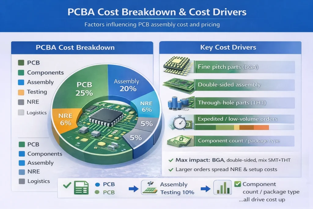
Core Cost Components
Material costs
PCB fabrication cost (material, layers, size, complexity, surface finish)
Component cost (often the biggest portion; scale affects unit price)
Assembly and processing costs
SMT placement and reflow
THT insertion and soldering (wave/selective/manual)
Additional processes (coating, cleaning, special handling)
Testing and quality control (often ~5–15%, varies by project)
AOI/AXI/ICT/FCT costs
Reliability testing (burn-in, environmental tests)
Engineering & service costs (variable)
NRE: stencil, fixtures, programming setup, special engineering work
Services: expedite premium, rework reserve, industry certification overhead (varies widely)
Main Cost Drivers
Component count and package types
Placement count impacts SMT cost. Tiny packages (01005/0201) and fine-pitch parts require higher precision and more setup time. BGA/QFN often adds X-Ray cost.
PCB design and process complexity
Double-sided assembly increases steps. Mixed SMT+THT increases workflow complexity and labor. PCB layers, minimum trace/space, hole density, blind/buried vias impact fabrication cost and yield.
Order volume and lead time
Volume drives unit cost via economies of scale. Rush lead times can increase cost due to capacity prioritization and constrained sourcing choices.
Practical Cost-Down Tips Without Sacrificing Quality
Apply DFM early: avoid extreme trace/space and overly dense via structures unless necessary
Simplify assembly: reduce THT where possible, minimize manual operations
Standardize parts and board formats to reduce procurement and setup time
Use smart panelization: improve throughput but weigh depaneling costs
Build a controlled substitution strategy to reduce shortages and price volatility
Consider turnkey PCBA (materials + assembly + testing) to reduce management burden and leverage factory sourcing scale
Quality Standards and Testing Options
Key Standards: IPC-A-610, J-STD-001, ISO 9001
IPC-A-610 defines acceptability criteria for assembled electronics (visual workmanship).
J-STD-001 specifies soldering requirements and process discipline (often paired with IPC-A-610).
ISO 9001 is a quality management system framework; it ensures structured management and continuous improvement via PDCA.
Depending on industry, additional certifications may apply (e.g., medical/automotive/aerospace), but requirements should be aligned with product risk level and customer compliance needs.
Inspection Methods: AOI vs X-Ray vs ICT vs FCT
AOI: fast visual inspection after soldering
X-Ray / AXI: required for hidden joints (BGA/QFN/CSP) and internal solder quality
ICT: checks net connectivity and basic component values
FCT: verifies full functional behavior under operating conditions
Reliability Options: Conformal Coating, Burn-in, Cleanliness Control
Conformal coating protects against moisture, dust, salt fog, chemicals, and corrosion
Burn-in screens early-life failures under stress
Environmental tests (e.g., high temp/humidity, thermal cycling) validate stability
Cleanliness control reduces ionic residues that can cause corrosion or electrochemical migration
Traceability & Documentation: Lot Tracking, Material Certificates, FA Reports
End-to-end lot tracking from PCB laminate and components to finished boards
Certificates of Conformance (CoC) / material certificates for critical parts
Failure analysis reports when issues occur
First article documentation and inspection summaries when required
How to Choose a Reliable PCBA Manufacturer
Capability Match
Minimum component size capability (e.g., 0201/01005)
Minimum pitch handling (e.g., fine-pitch QFP/BGA)
Typical FPY (First Pass Yield) metrics for comparable products
Special processes: conformal coating, selective soldering, BGA rework/reballing, programming
Component Sourcing & Anti-Counterfeit Process
Transparent sourcing channels and documented procurement process
Strong IQC and anti-counterfeit controls (inspection, traceability, verification)
Defined substitution approval workflow for alternates
Process Control
Full process coverage: IQC → SMT/DIP → multi-stage inspections → OQC
ESD controls aligned to recognized practices (and documented controls)
MSD management (storage, baking, floor-life tracking)
Reflow profile control and ongoing verification
Lead Time & Communication
Proactive DFM feedback before production
Clear ECO handling and revision control
Flexible planning for expedited builds
Responsive communication and defined after-sales support process
PCBA FAQs
Is PCBA the same as PCA?
Mostly yes. PCA (Printed Circuit Assembly) is another common term for assembled boards.
What’s the difference between SMT and PCBA?
SMT is one part of the PCBA process (surface-mount placement and soldering). PCBA includes SMT plus any through-hole work, inspection, testing, and packaging.
Can I buy components myself and send them to you?
Often yes. This is typically called consigned components. You’ll want clear rules for labeling, reels, MSD handling, and responsibility for shortages/DOA parts.
What if I don’t have a Pick & Place file or test requirements?
Many projects start that way. A manufacturer can often help generate or validate a placement file from your CAD outputs, and you can begin with AOI + basic power-on tests while you build a formal FCT plan.
How long does prototype vs production PCBA take?
It depends on PCB fabrication time, component availability, and test scope. Prototypes are often fastest with simplified testing; production adds fixture development and stronger controls.