PCBA Testing Methods: SPI vs AOI vs X-ray vs ICT vs Flying Probe vs FCT
Why PCBA Testing Is the Backbone of Quality Assurance
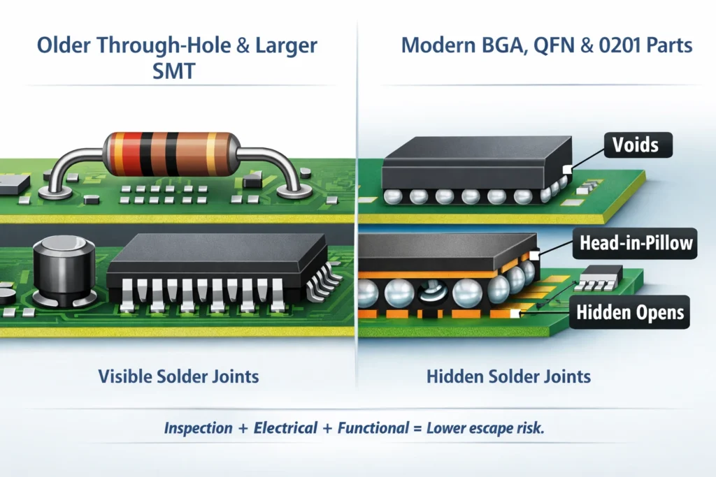
Why visual inspection is no longer enough
Visual inspection used to work when assemblies were larger and mostly through-hole. Today’s miniaturized designs—BGA/QFN packages, 0201 passives, fine-pitch ICs, and HDI routing—place critical solder joints where you simply can’t see them. Hidden interconnects mean a board can look perfect and still fail due to voiding, head-in-pillow, opens, or intermittent joints.
What “quality” means in practice
In PCBA manufacturing, quality is not a cosmetic score. It’s the ability to ship units that:
power on safely,
meet electrical specs consistently,
pass functional requirements under real I/O conditions,
remain reliable over time.
Testing is therefore a risk management system, not a checkbox.
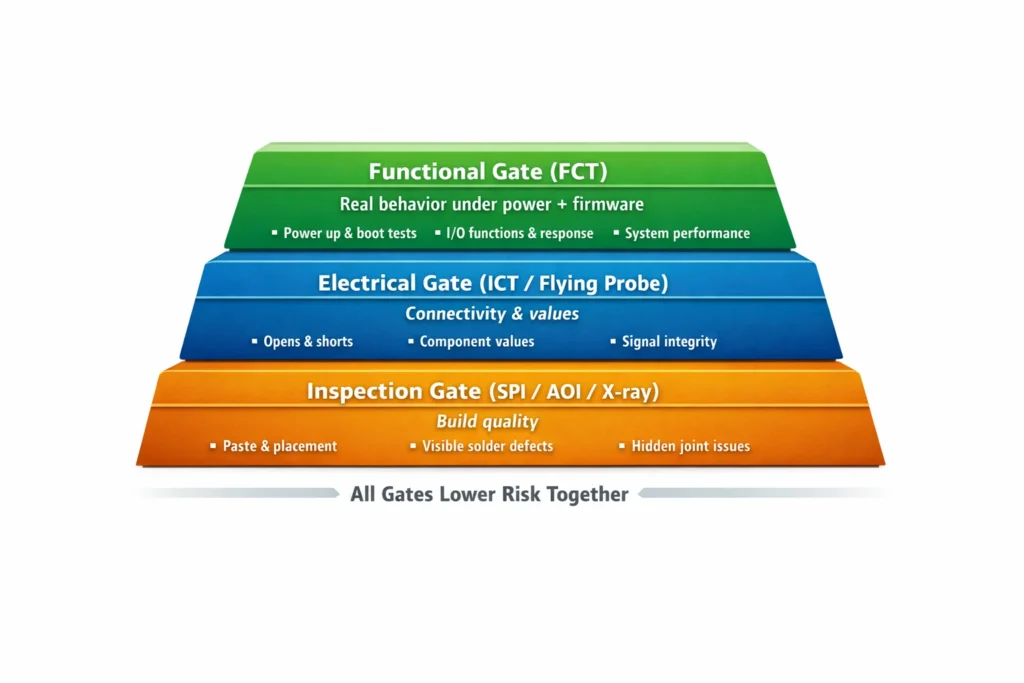
PCBA Testing vs Inspection vs QA
Inspection (SPI/AOI/X-ray) vs Electrical Test (ICT/Flying Probe) vs Functional Test (FCT)
Inspection tools (SPI, AOI, X-ray) verify physical build quality: paste deposition, component placement, polarity, visible solder, and hidden joint structure (via X-ray).
Electrical tests (ICT or flying probe) verify circuit integrity: opens/shorts and (often) component value checks.
Functional test (FCT) verifies real behavior: powering the assembly and checking performance under firmware and real I/O conditions.
What each method can/can’t prove
Inspection can confirm workmanship and many placement issues, but cannot prove connectivity or real function.
ICT/flying probe can confirm electrical integrity, but cannot validate firmware logic, timing margins, or full end-use behavior.
FCT can validate system behavior, but it depends on prior gates to reduce the risk of powering up a board with fundamental assembly faults.
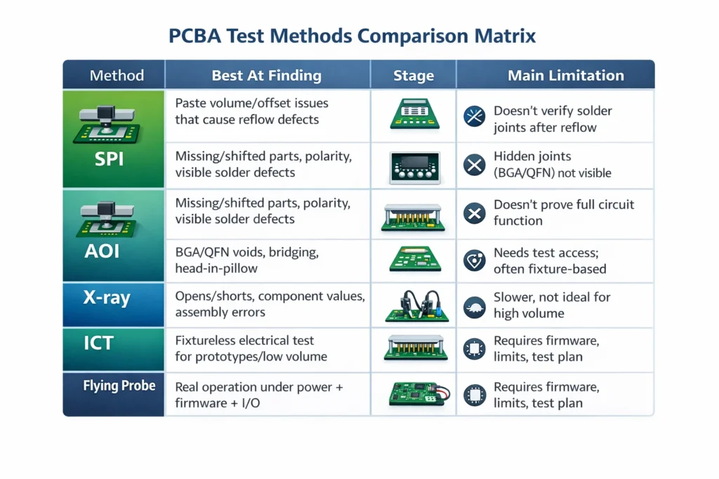
| Method | Best at finding | Typical stage | Main limitation |
|---|
| SPI | Paste volume/offset issues that cause reflow defects | Pre-reflow | Doesn’t verify solder joints after reflow |
| AOI | Missing/shifted parts, polarity, visible solder defects | Post-reflow | Hidden joints (BGA/QFN) not visible |
| X-ray | BGA/QFN voids, bridging, head-in-pillow | Post-reflow | Doesn’t prove full circuit function |
| ICT | Opens/shorts, component values, assembly errors | Post-assembly | Needs test access; often fixture-based |
| Flying probe | Fixtureless electrical test for prototypes/low volume | Prototype / low volume | Slower, not ideal for high volume |
| FCT | Real operation under power + firmware + I/O | Final QA | Requires firmware, limits, test plan |
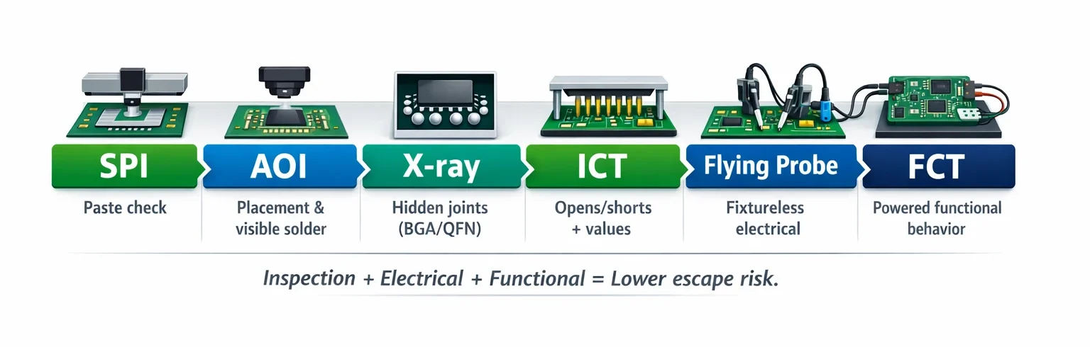
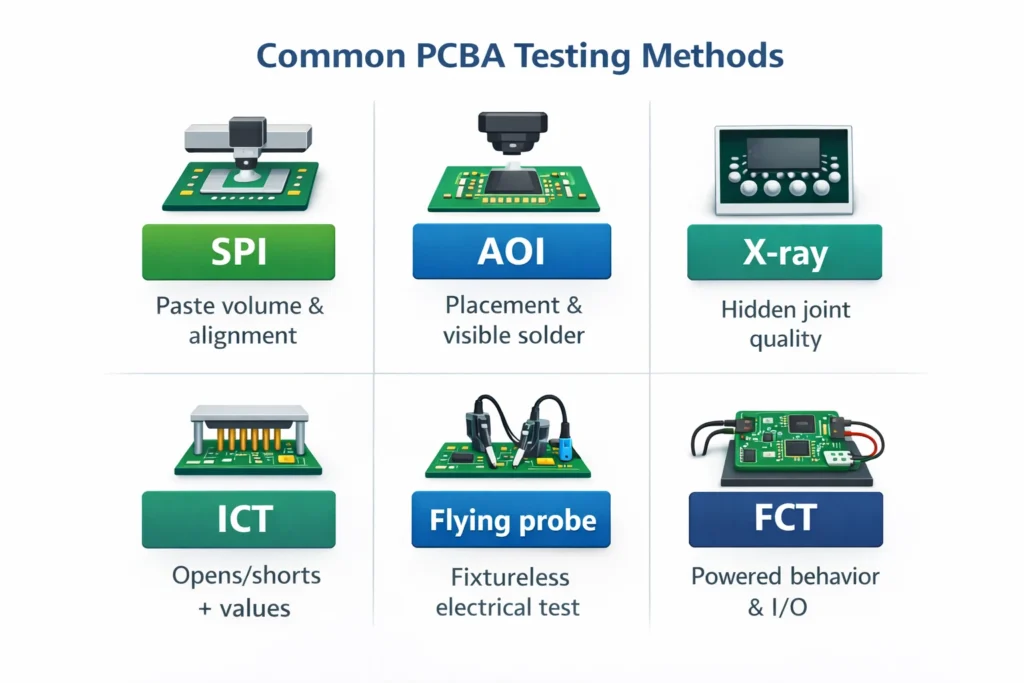
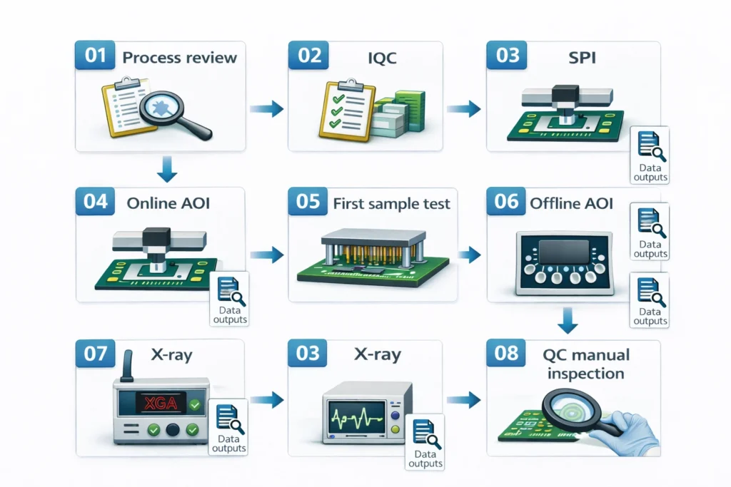
Common PCBA Testing Methods
SPI (Solder Paste Inspection)
Purpose: Detects insufficient/excess paste, misalignment, and bridging risk before reflow.
Why it matters: Fixing issues before reflow prevents expensive scrap/rework later.
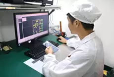
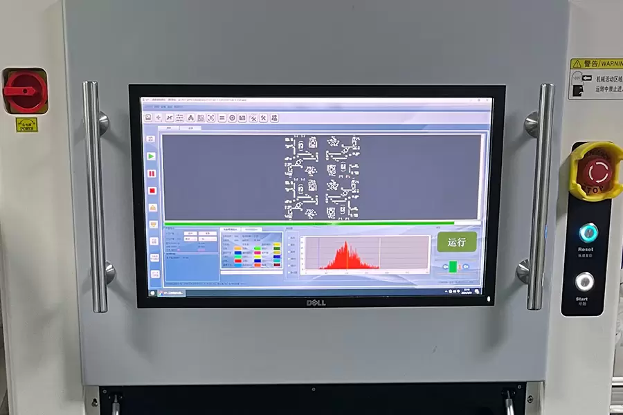
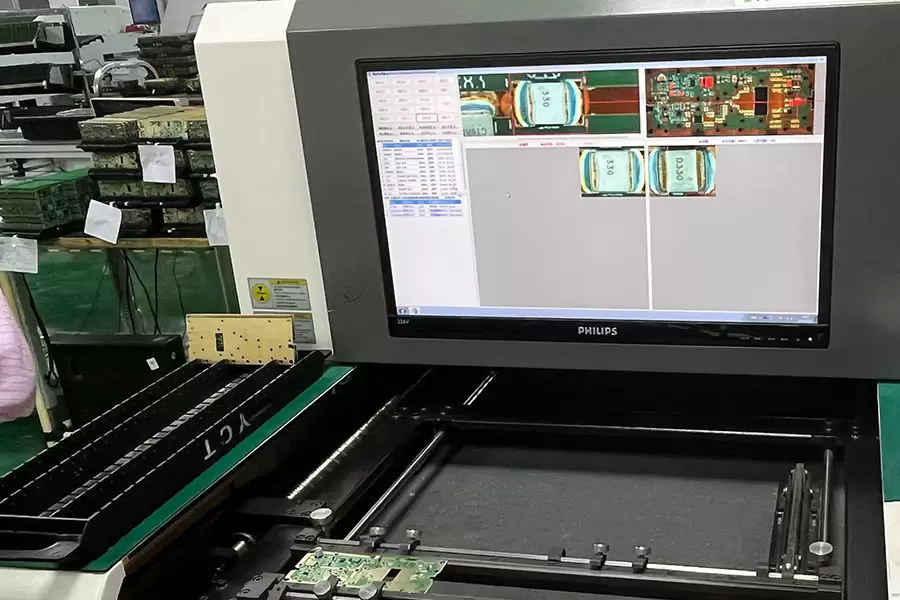
AOI (Automated Optical Inspection)
Purpose: Identifies missing parts, polarity errors, misalignment, tombstoning, solder bridges, insufficient solder fillets (where visible).
Why it matters: AOI is a fast, scalable screening gate for SMT quality.
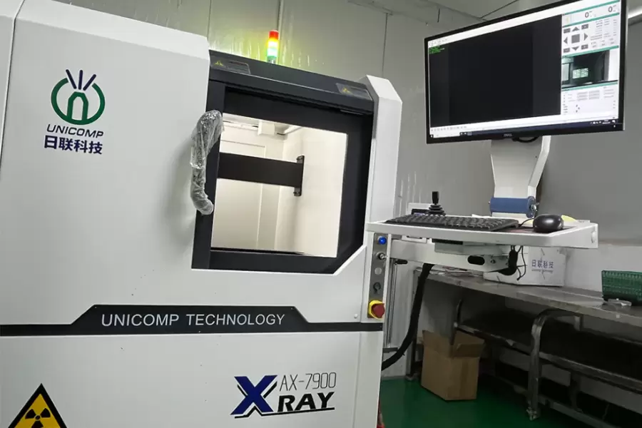
X-Ray Inspection
Purpose: Detects hidden solder joint problems under BGA/QFN/LGA packages: voiding patterns, bridging, head-in-pillow, insufficient wetting indicators.
Why it matters: X-ray is often the only practical way to inspect hidden joints without destructive analysis.
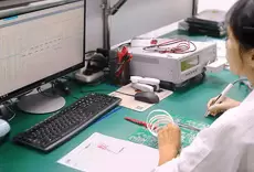
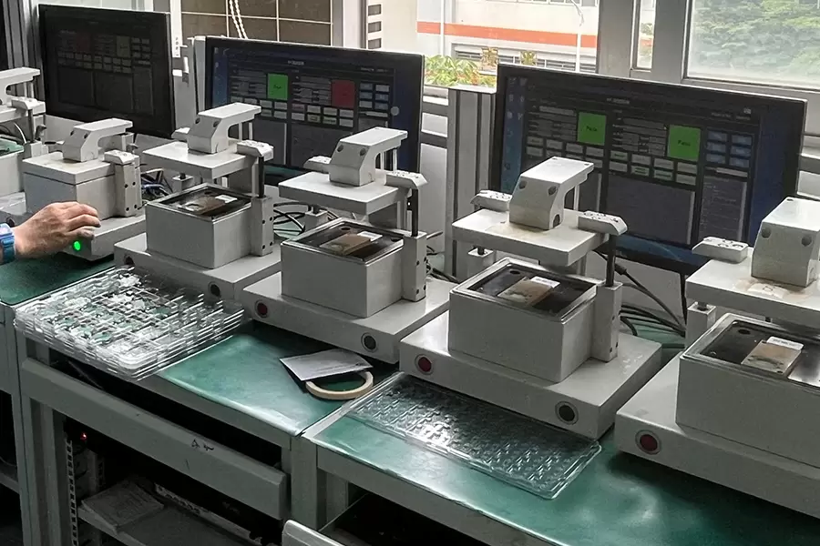
ICT (In-Circuit Test)
Purpose: Uses probing (often a bed-of-nails fixture) to access test points and verify opens/shorts, component values, orientation, and other electrical integrity checks.
Why it matters: ICT is extremely fast and repeatable in volume manufacturing—excellent as a production quality gate.
Flying Probe Test
Purpose: A fixtureless electrical test using moving probes—similar goals to ICT, but with flexible probing patterns.
Why it matters: Ideal for prototypes/NPI and small batches where fixture cost and lead time are not justified.
FCT (Functional Circuit Test)
Purpose: Powers up the board and verifies performance under firmware—interfaces, sensors, outputs, current draw, timing, and user-defined functional limits.
Why it matters: FCT provides the most direct evidence that a PCBA “works as intended,” which is often a key requirement for US/EU buyers.
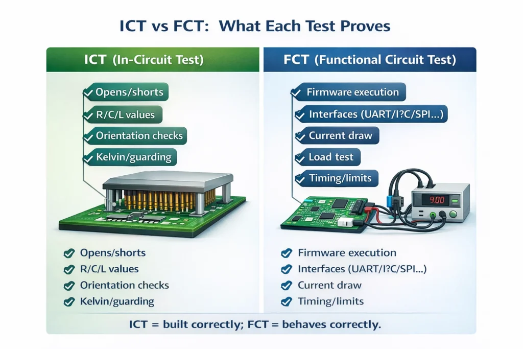
ICT vs FCT — Deep Technical Differences
What ICT really tests
ICT focuses on assembly-level electrical integrity:
opens/shorts between nets,
shorts to power/ground,
component value verification (R/C/L) within tolerance,
orientation checks for diodes/transistors and some pin-level tests,
guarding/Kelvin probing strategies for better measurement accuracy.
What FCT validates
FCT validates end-use behavior:
power sequencing and inrush/current draw limits,
stable rails under load,
firmware execution and logic checks,
interface verification (UART/I²C/SPI/CAN/USB/Ethernet/Wi-Fi as applicable),
sensor/actuator interaction, calibration verification, output drive capability.
Test coverage — why ICT + FCT together reduces risk
Using both dramatically reduces escapes because each method covers different failure modes.
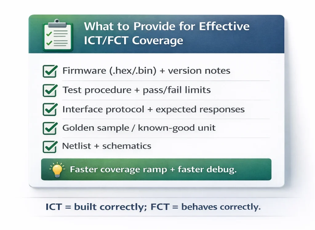
Inputs needed for success (what engineers should prepare)
To avoid delays and incomplete coverage, provide:
firmware (.hex/.bin) + version notes (or a test firmware variant),
test procedure + explicit pass/fail limits,
interface protocol details and expected responses,
golden sample / known-good unit,
netlist + schematics (helps boost electrical coverage and speed debug).
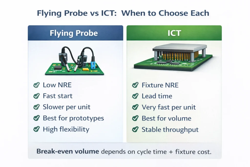
ICT vs Flying Probe
| Factor | Flying Probe | ICT (Bed-of-Nails) |
|---|
| Setup/NRE | Low | Medium–High (fixture + development) |
| Lead time | Fast to start | Fixture design/build required |
| Test speed | Slower per board | Very fast per board |
| Best for | Prototype / NPI / low volume | Mature design / mid–high volume |
| Flexibility | High | Fixed once fixture is built |
| Scalability | Limited | Excellent |
| Best outcome | Rapid iteration | Lowest long-run cost & stable throughput |
PCBA Testing Process in PCBAgroup
If Testing Finds Defects — Our Rework Process
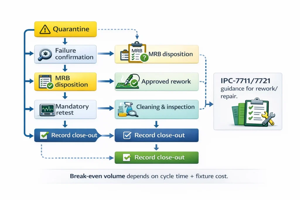
Rework policy overview
Quarantine & identification (hold area, clearly separated)
Failure confirmation & analysis (repeat test, isolate symptom)
MRB disposition (rework / component replacement / scrap / engineering review)
Approved rework by trained technicians
Cleaning & inspection (visual acceptability aligned to workmanship criteria)
Mandatory retest (same gate that caught the failure)
Record close-out (SN-linked rework history + retest results)
IPC-7711/7721 provides recognized guidance for rework, repair, and modification procedures for electronic assemblies.
How to Choose the Right Testing Strategy for Your Project
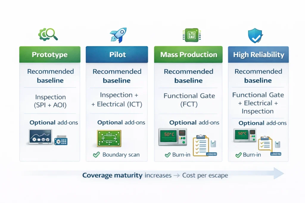
Prototype / NPI strategy
Goal: rapid learning and iteration.
Common approach: AOI + flying probe + basic FCT (often semi-automated).
Pilot run strategy
Goal: stabilize yield and lock in limits.
Common approach: AOI + (X-ray if needed) + flying probe or early ICT + stronger FCT.
Mass production strategy
Goal: throughput and consistency.
Common approach: AOI + ICT + FCT, often with integrated programming and parallel stations.
High-reliability strategy
Goal: minimize escapes and maximize documentation.
Add: X-ray for hidden joints, boundary scan where applicable, burn-in when required, stronger data logging.
| Project type | Recommended baseline | Optional add-ons |
|---|
| Prototype | AOI + Flying probe + basic FCT | X-ray for BGA/QFN, programming, boundary scan |
| Pilot | AOI + X-ray (as needed) + FCT | Start ICT planning if design stabilizes |
| Mass production | AOI + ICT + FCT | Burn-in, boundary scan, advanced traceability |
| High reliability | AOI + X-ray + ICT + FCT | Burn-in + stricter documentation + screening |
FAQ
How much does PCBA testing cost?
Cost depends on coverage, setup/NRE, cycle time, and volume. A practical way to estimate is:
NRE/setup: fixture + test development + program verification
per-unit test cost: cycle time × station capacity × yield impact
escape cost: returns and debug time if coverage is too low
Can you perform functional testing with custom firmware?
Yes—FCT usually requires your firmware (or a test build), interface protocol details, and clear pass/fail limits. It’s best to provide a golden sample and version notes so test logs match your configuration control.
Is 100% AOI enough for complex boards?
No. AOI is a strong inspection gate, but it cannot prove hidden joints or full electrical/functional behavior. Dense boards often require X-ray + electrical test (ICT/flying probe) + functional test (FCT) for high confidence.
What test data and traceability do you provide?
A professional deliverable includes SN-linked results, program revisions, firmware version, timestamps, and retest history. See the report template above.
What DFT changes will you recommend before production?
Common improvements include adding test points to critical nets, improving probe access, adding programming/debug pads, improving panelization alignment features, and (where applicable) boundary scan readiness.
Conclusion
What you get by working with PCBAgroup
ewer escapes and faster debug loops,
clearer documentation and traceability for audits,
smoother scale-up from prototype to mass production,
lower long-run cost through the right mix of methods.
To propose a practical test plan (AOI/X-ray/ICT/FCT), we recommend sending:
Gerber / fab files
BOM
Pick & Place (XY)
Schematic + netlist (if available)
Firmware/programming notes (if FCT or programming is required)
Key performance limits / acceptance criteria (what must be verified)
We’ll reply with a recommended strategy, expected lead time drivers (fixture/test development), suggested DFT improvements, and a sample deliverables package.