Table of Contents
What Is a Rigid PCB? Types, Materials, Specs, Cost & Supplier Checklist
A Rigid PCB (Rigid Printed Circuit Board) is the most widely used type of printed circuit board in electronic products. Its core feature is a hard, non-bendable base material, which provides stable mechanical support and reliable electrical interconnection for components. Rigid PCBs achieve these connections by etching copper circuitry on a rigid insulating substrate.
If you’re an engineer designing a board—or a procurement team sourcing one—this guide explains what a rigid PCB is, how it differs from other PCB types, which specifications actually matter, and how to avoid surprises in quoting and manufacturability (DFM).
Key Takeaways
Rigid PCBs are the default choice for most products because they balance cost, manufacturability, and reliability.
The biggest drivers of price and lead time are usually layer count, material type, feature sizes, via structures, and surface finish.
A good rigid PCB build starts with the right inputs: Gerber/ODB++, drill files, stackup/impedance requirements, surface finish, thickness, copper weight, IPC class, and quantity.
Use specialty rigid variants (High-Tg, heavy copper, metal core, high-frequency laminates) only when the requirements justify them.
What Is a Rigid PCB?
A rigid PCB is created by etching copper foil on a rigid insulating substrate (most commonly FR-4). For multilayer boards, additional layers are formed through lamination, drilling, plating, and imaging processes.
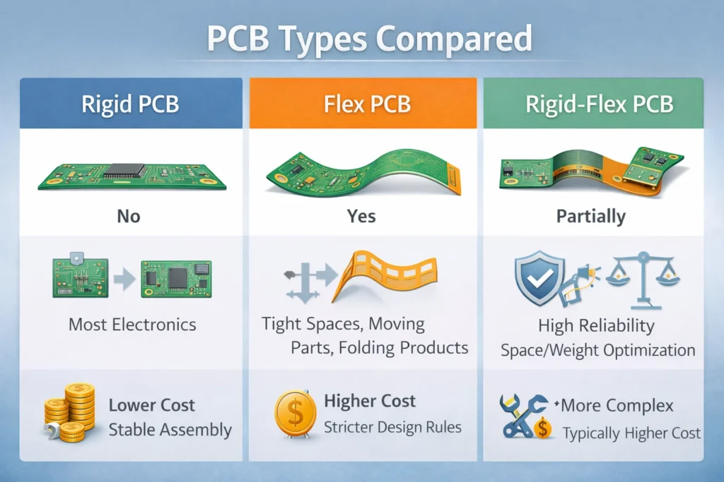
Rigid PCB vs Flex PCB vs Rigid-Flex PCB
| PCB Type | Can it bend? | Best for | Typical tradeoff |
|---|---|---|---|
| Rigid PCB | No | Most electronics, stable assemblies, scalable volume | Not suited for fold/3D routing |
| Flex PCB | Yes | Tight spaces, moving parts, folding products | Higher cost, stricter design rules |
| Rigid-Flex PCB | Partially | High reliability + space/weight optimization | More complex, typically higher cost |
If your design does not require bending, a rigid PCB is usually the most cost-effective and scalable option.
Practical rule: Choose rigid unless flexibility is functionally necessary.
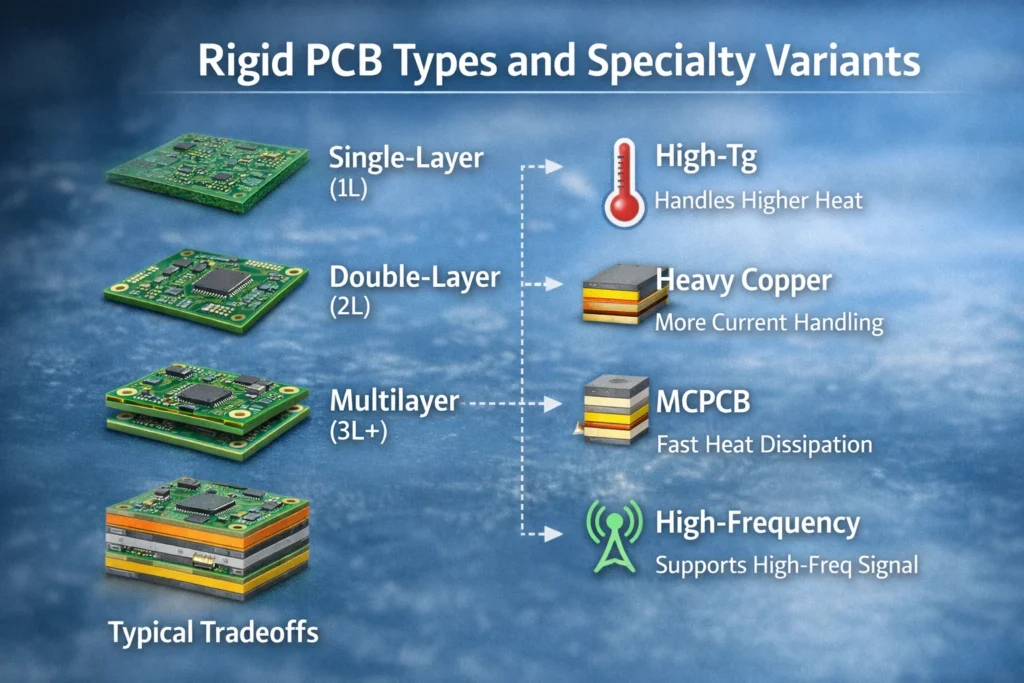
Common Types of Rigid PCBs
Single-Layer (Single-Sided) Board
Made of one insulating substrate with copper on one side. Because routing is only possible on a single surface, it is low-cost and simple to manufacture.
Common uses: basic electronics, calculators, LED lighting boards.
Double-Layer (Double-Sided) Board
Copper exists on both sides of the substrate. Routing and component placement can be done on both sides, offering more routing area and supporting moderately complex circuits.
Common uses: medium-complexity electronics.
Multilayer Board
Built by laminating three or more copper layers with insulating materials in between, connected by through vias, blind vias, or buried vias.
Advantages: higher routing density, improved signal integrity, better EMI resistance, and dedicated power/ground planes.
Common uses: complex devices requiring performance, reliability, and miniaturization.
Specialty Rigid PCBs
Metal Core PCB (MCPCB)
Uses a metal base (commonly aluminum or copper) for excellent heat dissipation.
Common uses: LED lighting, power amplifiers, power modules.
High-Frequency PCB
Uses special low-loss substrate materials to support high-frequency signal transmission.
Common uses: wireless communications, radar, satellite communications.
High-Tg Rigid PCB
High-Tg materials maintain mechanical stability at higher temperatures and tolerate greater thermal stress during soldering.
Common uses: automotive electronics, industrial equipment, some high-end consumer electronics.
Heavy Copper Rigid PCB
Uses thicker-than-standard copper to carry higher current and improve heat spreading.
Common uses: DC-DC converters, motor controllers, power modules, automotive power systems.
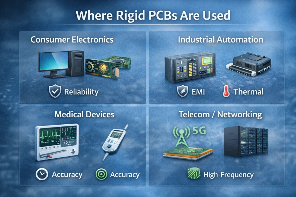
Typical Applications of Rigid PCBs
Consumer electronics: motherboards, graphics cards, memory modules, chargers
Communication & networking: RF transmitters/receivers, high-performance systems; 5G infrastructure and servers often use multilayer rigid PCBs
Industrial control & automation: PLCs, inverters, servo drives, HMIs, instrumentation boards
Automotive electronics: ECU, BMS, ABS/ESP, sensor modules (pressure/temperature, etc.)
Medical devices: ECG, blood pressure/thermometers, imaging systems (CT/MRI), IVD instruments, sequencing equipment (requirements depend on product and compliance pathway)
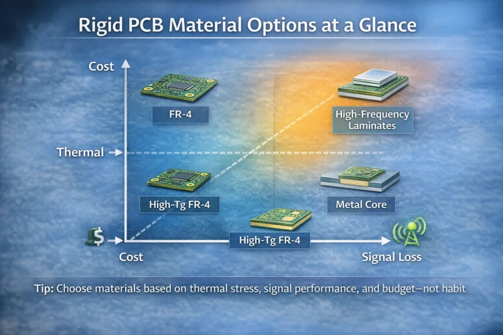
Key Materials Used in Rigid PCBs
FR-4
The most common rigid PCB substrate. FR-4 is a composite of epoxy resin and fiberglass cloth. Fiberglass provides strength and dimensional stability; epoxy provides insulation and flame resistance.
Typical use: low-to-mid frequency, low-to-mid power applications across many industries.
High-Tg Materials
Provide improved dimensional stability, heat resistance, moisture resistance, and chemical resistance under higher-temperature processes (e.g., lead-free reflow).
Typical use: high-density assembly, boards requiring better thermal robustness.
High-Frequency / High-Speed Laminates
At higher frequencies, FR-4 dielectric loss can increase. Low-loss materials (e.g., PTFE, ceramic-filled laminates, PPO/PPE systems) may be used when signal performance requires it.
Metal Substrates (Aluminum / Copper Core)
Typically consist of a metal plate, dielectric insulating layer, and copper foil.
Primary advantage: heat dissipation.
Copper Foil (ED vs RA)
ED copper: cost-effective and common for general rigid PCB use
RA copper: smoother surface and better ductility; often discussed in high-frequency signal performance or flexible circuits
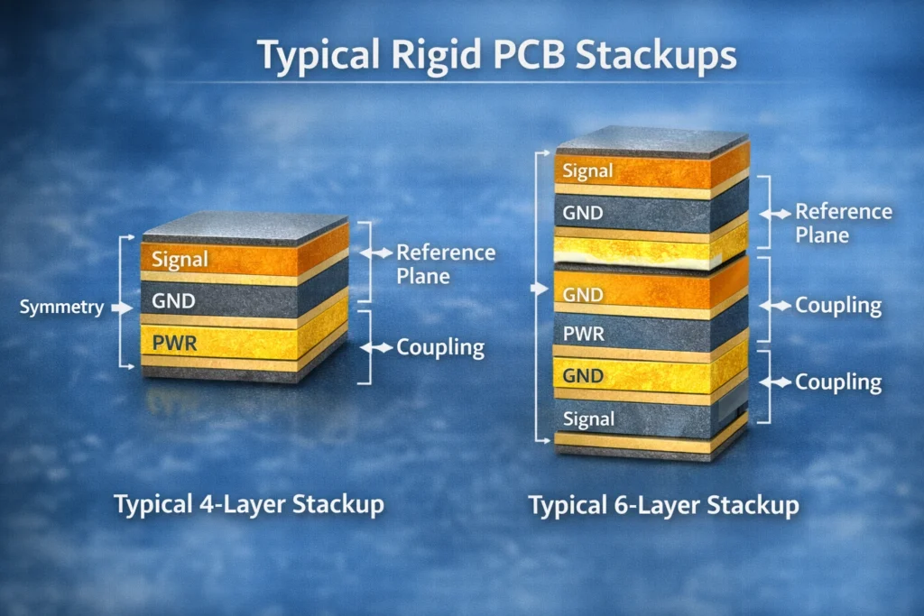
Layer Count and Stackup Structure
Layer Definitions
Single-sided: routing on one side
Double-sided: routing on both sides, connected by vias
Multilayer: stacked inner cores and prepregs (PP), interconnected by through/blind/buried vias
Increasing layers can improve power distribution, reduce crosstalk, suppress EMI, and support high-speed signal transmission.
Stackup Design Rules (Signal + Power Integrity)
Symmetry: a symmetric stackup helps balance lamination stress and reduce warpage
Tight coupling: keep power and ground planes close for better decoupling
Reference planes: place signal layers near a continuous reference plane to support clean return paths
Adjacent signal layers: increase spacing and route orthogonally where practical to reduce crosstalk
Copper Weight and Its Impact on Performance
Current capacity: thicker copper increases current-carrying capability
Thermal performance: copper spreads heat; thicker copper can reduce local hot spots
Signal integrity (high frequency): due to skin effect, current flows mainly on the surface; excessive copper thickness can be unhelpful and may increase loss if roughness becomes a factor
Board weight: copper weight affects total board weight; weight-sensitive designs may use regional copper strategies or wider traces instead of heavier copper
Combined effect with board thickness: total board weight depends on laminate thickness + copper weight; designers balance structural strength and electrical needs
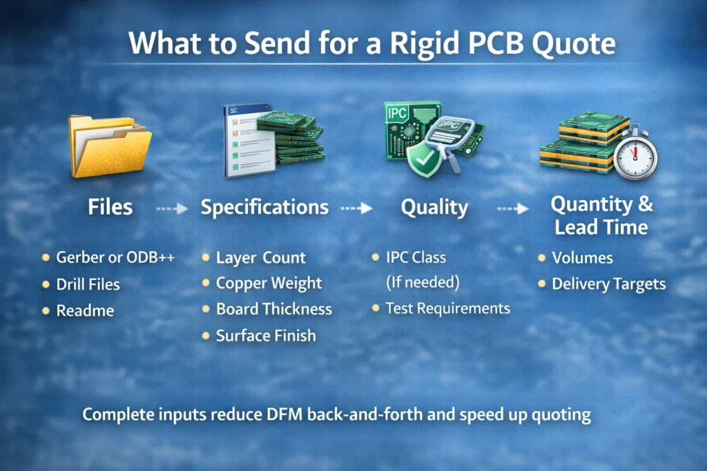
Quoting-Critical Rigid PCB Specifications (What You Must Provide)
If you want a fast, accurate quote and fewer DFM loops, these parameters are essential.
Core Build Parameters
Layer count and target stackup
Board thickness (and critical tolerances, if needed)
Copper weight (inner/outer if different)
Solder mask + silkscreen requirements
Surface finish
DFM-Critical Feature Constraints
Minimum trace/space
Minimum finished hole size
Annular ring requirements
Via type (through / blind / buried / microvia if needed)
Impedance control targets and constraints (reference layers, tolerance)
RFQ Checklist
| Category | What to provide | Why it matters |
|---|---|---|
| Files | Gerber or ODB++, drill files, readme | Prevents missing data and quote delays |
| Stackup | Layer count, thickness, copper weight | Determines manufacturability and cost |
| Finish | ENIG/HASL/OSP/etc. | Affects assembly, shelf life, cost |
| DFM limits | Trace/space, hole size, annular ring | Controls yield and feasibility |
| Impedance | Targets + reference layers | Needed for accurate build |
| Quality | IPC class (if applicable), test requirements | Aligns acceptance and inspection |
| Quantity + lead time | Volumes + delivery targets | Impacts pricing and scheduling |
Vias: Through Vias vs Blind/Buried Vias
Vias are the core structures that connect electrical signals between layers:
Through vias (PTH): go from top to bottom; mature process; cost-effective
Blind vias: connect outer layers to inner layers; save routing space; used in high-density designs
Buried vias: exist only inside the PCB; connect inner layers; maximize outer-layer routing space
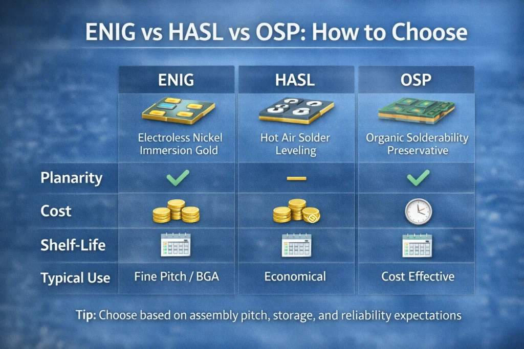
Surface Finish: ENIG, HASL, and OSP
Surface finish selection depends on assembly method, pitch, storage, and reliability goals:
ENIG: flat finish, widely used for fine pitch/BGA; usually higher cost
HASL: economical and common; planarity may matter for very fine pitch
OSP: cost-effective with good solderability; handling and shelf-life considerations apply
Immersion silver/tin and others: used for specific requirements—evaluate with your supplier and assembly process
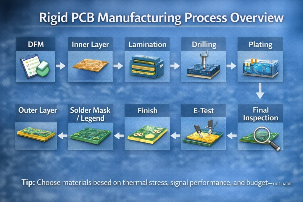
Rigid PCB Manufacturing Process
1) File Review + DFM Preparation
After receiving design files, the engineering team conducts a DFM review to confirm manufacturability within factory capability. Material, stackup, copper thickness, and production panel format are planned.
2) Inner Layer Circuit Fabrication
Large copper-clad panels are cut to production sizes. The surface is prepared (brushing/micro-etch) to improve adhesion.
A dry film photoresist is applied; the circuit image is transferred by UV exposure. After developing, unwanted copper is etched away, and the resist is stripped. Inner layers are typically inspected by AOI.
3) Lamination
Oxidized inner layers, prepregs (PP), and outer copper foils are stacked in the designed order. The stack is pressed under controlled temperature and pressure (often vacuum lamination).
4) Drilling + Hole Metallization
CNC drilling creates through/blind/buried vias (as designed). Layer alignment may be verified (e.g., X-ray for certain builds).
Hole walls are treated to remove resin smear and improve adhesion.
An electroless copper process deposits a thin conductive layer; then electroplating thickens copper in holes and on surfaces to meet requirements.
5) Outer Layer Circuit + Surface Finish
Outer layers are patterned using similar imaging steps. Copper is built up where required, protected during etching, then final outer circuitry is formed.
Solder mask is applied and cured, and legend markings are printed. Pads receive the specified surface finish (HASL, ENIG, immersion silver, OSP, etc.).
6) Profiling + Final Inspection
Boards are routed/V-cut to final outline. Electrical testing (flying probe or fixture) verifies connectivity (no opens/shorts). A final visual/measurement inspection confirms appearance, size, and hole positions before packaging.
Reliability Considerations
Warpage Control (Critical for BGA / Fine Pitch)
Larger board size, unbalanced copper distribution, and certain stackups can increase warpage risk. A symmetric stackup and balanced copper distribution help reduce it.
Thermal Stress and Delamination Risk
High-Tg materials and stable lamination processes can reduce risk in harsh thermal cycling.
CAF and Insulation Integrity
Spacing rules, cleanliness, materials, and process controls all impact long-term insulation reliability.
IPC Class (Class 2 vs Class 3)
IPC class defines acceptance criteria and inspection strictness. Select it based on reliability requirements and budget.
Cost Drivers for Rigid PCBs (and Practical Cost-Down Levers)
Biggest Cost Drivers
Layer count (more inner layers + lamination steps)
Specialty materials (High-Tg, RF/low-loss laminates, metal core)
Tighter features (trace/space, drill size, annular ring constraints)
Complex via structures (blind/buried/microvias, via-in-pad)
Surface finish and special requirements
Testing/inspection requirements (project-defined)
Practical Ways to Reduce Cost (Without Quality Risk)
Use the lowest layer count that meets routing + EMI needs
Avoid HDI unless it significantly reduces size or layers
Stick to standard thickness/materials/finishes when possible
Reduce unnecessary drill variants and overly strict rules
Improve panel efficiency through smart panelization (ask your supplier)
Factors That Affect Lead Time
Lead time depends on complexity and scheduling. Common delay causes include:
special laminate availability
HDI or multiple lamination cycles
stackup/impedance validation loops
unusually tight tolerances or special tests
Fastest path: send complete files/specs, respond quickly to DFM questions, and keep materials/finishes standard unless needed.
How to Choose a Rigid PCB Manufacturer
Capability Checklist
Meets requirements for trace/space, holes, layers, thickness
Experience with impedance control (if needed)
Can scale consistently from prototypes to mass production
Quality & Process Checklist
Clear inspection options (AOI/electrical test)
Traceability and documentation aligned with your industry
Transparent, actionable DFM feedback
Communication Checklist
Speed and clarity of DFM feedback
Ability to propose cost-down alternatives without harming function
Stable point of contact that aligns engineering and procurement
How to Get a Fast, Accurate Quote
Send:
Gerber or ODB++ files, drill files, readme
Quantity and target delivery
Material preference (or “FR-4 unless otherwise required”)
Board thickness and copper weight
Surface finish and solder mask requirements
IPC class requirement (if applicable)
Impedance requirements (targets, reference layers, constraints)
Special notes (edge fingers, controlled depth routing, via-in-pad, etc.)
Ready to start your rigid PCB project? Share your design files and requirements and request a DFM review + quotation to confirm manufacturability, cost drivers, and lead time before production.
FAQ
What are rigid PCBs used for?
Most electronics use rigid PCBs because they provide stable assembly, consistent mechanical fit, and scalable manufacturing from prototypes to mass production.
Is FR-4 always the best choice?
FR-4 is the most common default material. High-Tg or specialty laminates are used when thermal or signal performance requirements are higher.
When do I need controlled impedance?
High-speed interfaces and RF circuits often require controlled impedance because reflections and loss can affect performance. Provide impedance targets and stackup context for accurate manufacturing.
What’s the difference between through vias and blind/buried vias?
Through vias go from top to bottom and are cost-effective. Blind/buried vias improve routing density but increase process complexity and cost.
Which surface finish is best for BGA?
Many teams choose flatter finishes for fine pitch/BGA assembly, but the best choice depends on assembly process, storage conditions, cost, and reliability goals.