Table of Contents
What Is SMT (Surface Mount Technology) Assembly?
If you’re sourcing PCB assembly (PCBA), you’ll quickly see “SMT” on quotes, capability lists, and process documents. But SMT isn’t just a term—it directly affects cost, lead time, yield, and product reliability.
This guide explains:
What SMT is (in plain English)
SMT vs THT (through-hole) and when each makes sense
The full SMT process—from DFM to SPI/AOI/X-ray/ICT/FCT
What data you must send for an accurate quote
How to evaluate a PCBA supplier with less risk
What is SMT
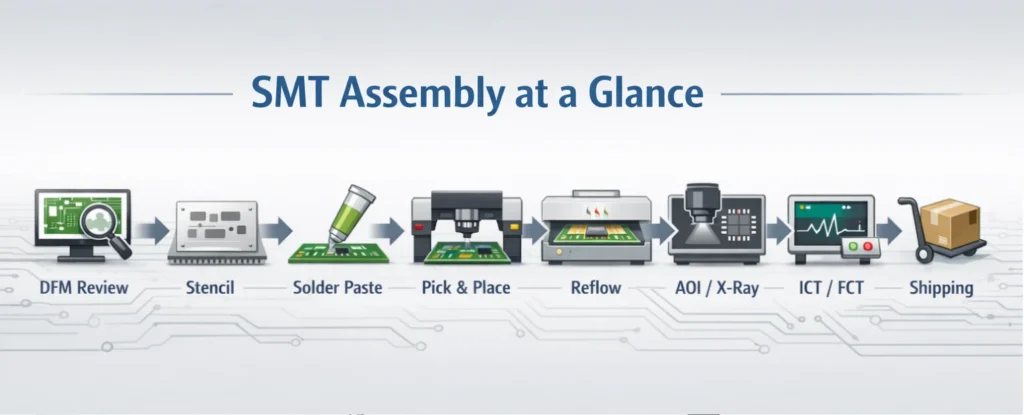
SMT (Surface Mount Technology) is a PCB assembly method where components are mounted directly on the surface of the PCB. The typical sequence is solder paste printing → component placement → reflow soldering, followed by inspection and testing.
Quick terminology:
SMT = the assembly process/technology
SMD = surface-mount components (chip resistors/caps, QFN, BGA, etc.)
PCBA = the assembled circuit board (PCB + components + solder + test)
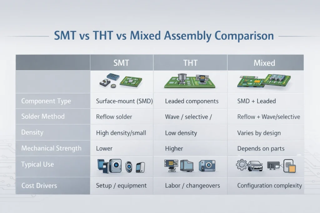
SMT vs THT
Many buyers still use “DIP” as a general label for plug-in assembly, but for international customers, the clearest comparison is SMT vs THT (through-hole technology).
Core differences
SMT: Uses SMDs mounted on the PCB surface, soldered mainly by reflow. Ideal for high density and automation.
THT: Uses leaded components inserted into drilled holes, soldered by wave/selective soldering or hand solder. Often chosen for mechanical strength (connectors, large components).
When SMT is usually the best choice
Compact products (consumer electronics, portable devices)
High component density and fine-pitch packages
Designs requiring efficient volume production
When THT still matters
High mechanical stress connectors
Certain power/magnetic components
Designs that need stronger pin anchoring
The SMT Assembly Process
A strong SMT supplier doesn’t just run a line—they manage risk through defined quality gates. Here’s the buyer-relevant view of the process.
1) Engineering review / DFM (Design for Manufacturability)
Before production starts, a good factory checks:
BOM/CPL alignment and revision control
Polarity, reference designators, package orientation
Panelization, tooling, fiducials, keepouts
High-risk packages (BGA/QFN/LGA, fine pitch) and test approach
Buyer tip: DFM is the cheapest place to fix problems.
2) Stencil fabrication
The stencil (steel mesh) controls solder paste volume and shape. Poor stencil design can increase bridging, opens, and rework.
3) Solder paste printing
Printing quality strongly affects yield. Key controls include:
print pressure/speed, separation settings
PCB support tooling
stencil cleaning frequency
4) SPI (Solder Paste Inspection)
SPI checks paste volume/height/area before placement—often the most effective gate to prevent downstream defects.
5) Pick-and-place
Placement accuracy, feeder condition, nozzle condition, and vision calibration matter—especially for small passives and fine pitch.
6) Reflow soldering (profile control)
Reflow forms the solder joints permanently. Profile tuning must match:
solder paste type
PCB copper balance / warpage risk
package thermal mass (BGA, QFN thermal pads)
7) AOI / X-ray inspection
AOI catches visible issues: missing parts, polarity, tombstoning, misalignment, many solder appearance defects.
X-ray is critical for hidden joints (BGA/CSP/QFN/LGA) to assess voiding, bridging, opens.
8) ICT / FCT and programming (as required)
ICT verifies electrical connectivity and component values via test points (usually fixture-based).
FCT validates real functional behavior under power and signals (product-like environment).
9) Rework + final QC + packing
Controlled rework procedures, final inspection, ESD-safe packaging, labeling and traceability close the loop.
Common SMT Defects
From a buyer perspective, defects matter because they cause rework, schedule slips, and field failures.
Typical examples:
Solder bridging (often paste/stencil/process related)
Tombstoning (small passives, pad/thermal imbalance)
Voiding (thermal pads, paste/profile related)
Non-wet opens / head-in-pillow (often BGA/warpage/process window)
What you should ask your supplier: Which gates (SPI/AOI/X-ray/test) are used for your specific risks, and what evidence/reporting you’ll receive.
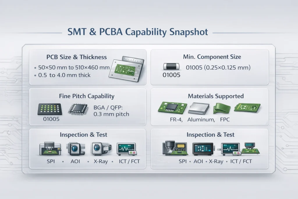
PCBAgroup Capability Snapshot
For international buyers, “capability” must be specific. Here are example measurable items from an SMT capability sheet:
- PCB size range: 50×50×0.5 mm up to 510×460×4.0 mm.
- Max PCB weight: 2.0 kg.
- Supported materials: FR-4, CEM-1, CEM-3, aluminum-based board, FPC.
- Surface finish examples: HAL, OSP, immersion gold, flash gold, gold finger.
- Minimum chip size example: 01005 (0.25×0.12).
- BGA pitch range example: 0.3–1.0 mm; QFP pitch 0.3–1.0 mm.
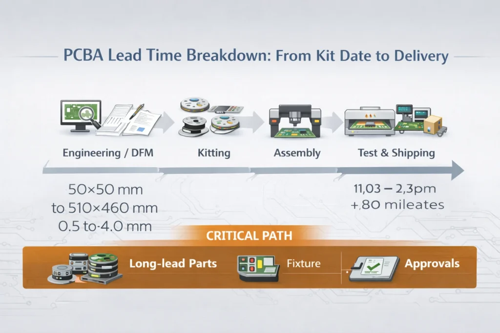
Lead Time: What’s Normal, What Causes Delays
In real projects, lead time is rarely limited by line speed. It’s usually driven by:
component availability and kitting readiness (kit date)
engineering questions (DFM, missing data)
test fixture or programming requirements
customer approval gates (FAI, test sign-off)
Some capability sheets provide assembly-time estimates only (excluding PCB fabrication and component procurement). For example, one lead-time table explicitly notes: “The above lead time is just for assembly time.”
Sample assembly-time entries include:
- SMD + connector: 5–200 pcs, normal 6 WD, quick-turn 3 WD
- SMD + DIP: 5–200 pcs, normal 5 WD, quick-turn 4 WD
- SMD + DIP: ≥2000 pcs, normal 8 WD, quick-turn 6 WD
A practical way to communicate schedule:
Delivery date = Kit date + Assembly time + Test/packing + Transit time
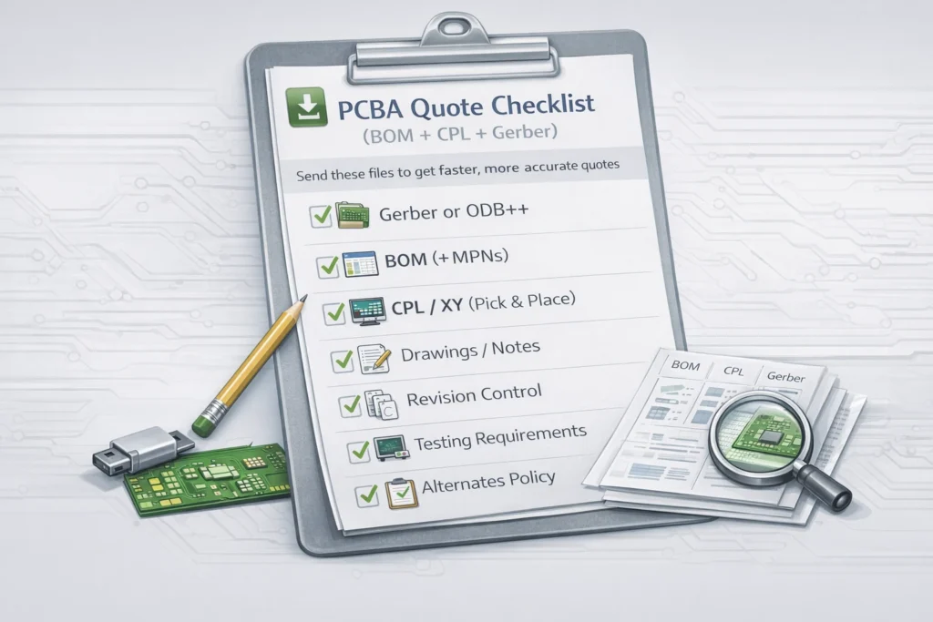
What to Send for a Fast, Accurate SMT Quote
Manufacturing data (PCB)
Gerber or ODB++
stack-up (if impedance control/special materials apply)
fabrication notes/drawings
Assembly data (SMT)
BOM with MPNs, package, quantity, and approved alternates/AVL
CPL/XY placement file (rotation, side, reference designators)
assembly drawing (polarity, critical notes, connector instructions)
Revision control + substitutes policy
confirm PCB/BOM/CPL are the same revision
specify “no substitutes” vs “approved alternates only”
Test and acceptance requirements
ICT/FCT/programming needs
expected coverage or pass criteria
FAI/sample requirements and any required reports
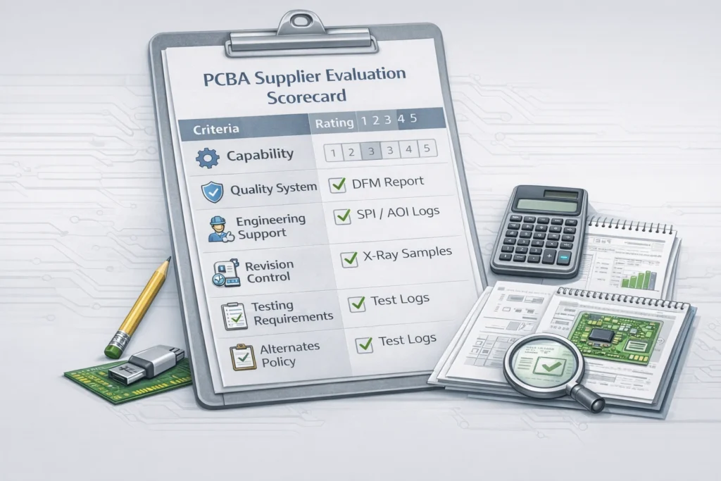
How to Choose a PCBA Supplier
1) Hardware and process capability (fit + repeatability)
minimum package/pitch that matches your design
reflow, wave/selective solder for mixed builds
availability and usage policy of SPI/AOI/X-ray/testing
2) Engineering and quality system (people + process)
DFM review ownership and response speed
IQC/IPQC/OQC flow and escalation method
structured root-cause actions for defects (e.g., 8D-style discipline)
3) International communication and logistics
English technical support and documentation
time-zone response plan
shipping experience and packaging/labeling discipline
4) Validate with a pilot order
build quality and yield
documentation/reporting
responsiveness and change control
FAQ
Do I need X-ray for my PCB assembly?
If your board uses hidden-joint packages like BGAs, X-ray is often the most reliable way to verify solder joint integrity beyond what AOI can see.
Why does my quote change after production starts?
Common reasons include BOM/placement revision mismatch, unclear alternates policy, missing programming files, or test requirements discovered late.
Is SMT reliable for industrial products?
Yes—when DFM, process control (printing + reflow profile), and inspection/testing strategy match the risk level of the product and environment.
To request an SMT/PCBA quote, send:
Gerber/ODB++ + BOM (with MPNs) + CPL/XY + revision info + test/acceptance requirements + alternates policy.
If you prefer, we can start with a DFM review to identify risk points before you commit to production.