
Table of Contents
BGA PCB Assembly Guide: DFM, X-Ray Inspection, Rework, Cost and RFQ Checklist
BGA PCB assembly is not simply standard SMT assembly with a more complex package.
For engineers and procurement teams, BGA changes the risk profile of a printed circuit board assembly. The solder joints sit under the package body. Visual inspection cannot verify every ball. A small weakness in pad design, via-in-pad treatment, solder paste volume, component moisture control, PCB flatness, reflow profiling, inspection scope, or test coverage can decide whether a build runs cleanly or enters a costly rework loop.
That is not an argument against BGA packages. Ball grid array packages make compact, high-I/O, high-speed, high-density electronics practical. SoCs, FPGAs, memory devices, RF modules, communication chips, embedded computing modules, power-management ICs, and advanced industrial control boards often depend on BGA, CSP, LGA, QFN, or other fine-pitch packages.
The risk appears when planning is weak.
If the PCB design, RFQ package, assembly capability, X-ray inspection scope, functional test plan, and acceptance criteria are not aligned before production, the buyer may discover the issue only after the first build. At that stage, every correction is slower: DFM clarification, stencil change, reflow adjustment, extra X-ray review, BGA rework, functional debug, or even PCB redesign.
This guide looks at BGA PCB assembly from the buyer’s side. It is written for hardware engineers, NPI teams, electronics OEMs, and procurement teams that need to know what to check before requesting a quote, how to reduce hidden solder joint risk, what X-ray inspection can and cannot prove, when BGA rework is realistic, what drives cost and lead time, and what belongs in a BGA assembly RFQ.
Quick Answer: What Should Buyers Check Before BGA PCB Assembly?
Before placing a BGA PCB assembly order, align on BGA pitch, PCB stack-up, material, surface finish, via-in-pad treatment, solder mask design, stencil strategy, X-ray requirements, test criteria, reliability level, batch quantity, and rework policy.
Use the table below as a practical starting point.
| Check item | Why it matters | What buyers should provide or confirm |
|---|---|---|
| BGA pitch and ball count | Fine pitch leaves less process margin for paste printing, placement, and inspection | BGA datasheet, package drawing, ball map, pitch, package size |
| PCB stack-up and material | Asymmetric stack-ups, thin cores, heavy copper, or large panels may increase warpage risk | Stack-up drawing, board thickness, copper weight, material requirements |
| Surface finish | Fine-pitch BGA often needs good flatness and solderability | ENIG, ENEPIG, OSP, HASL, or other finish requirement, confirmed with supplier |
| Via-in-pad | Unfilled or poorly planarized vias can wick solder and create weak joints or voiding | VIP locations, filled/capped via requirements, fabrication notes |
| Solder mask design | Mask registration and mask bridge width affect bridging risk and pad definition | Gerber/ODB++, solder mask layer, fabrication drawing |
| Stencil strategy | Paste volume affects opens, bridging, voiding, and ball collapse consistency | Paste layer, BGA package data, any step stencil requirement |
| SPI / paste inspection | Detects paste volume, height, area, and offset before placement | Whether SPI is required for BGA/QFN pads |
| X-ray inspection | Hidden solder joints cannot be fully checked by AOI or visual inspection | 100% or sampling, 2D or advanced inspection need, report expectations |
| ICT / FCT / programming | X-ray does not prove product function | Test procedure, firmware, pass/fail criteria, fixture notes |
| Quantity and forecast | Prototype and production have different cost and test economics | Prototype, pilot, production quantity, forecast |
| Acceptance criteria | Prevents disputes about voiding, rework, reports, and shipment approval | IPC class, customer criteria, report and rework rules |
For simple prototypes, the discussion can be lighter. For fine-pitch BGA, double-sided SMT, HDI routing, high-reliability products, industrial electronics, medical electronics, communication modules, or long-life equipment, the RFQ should be more detailed.
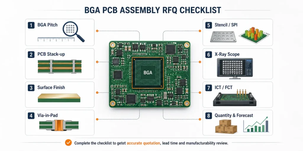
Key Checks Before Quotation
A useful BGA assembly quote should not be built from Gerber files and a BOM alone. The supplier should understand:
- BGA package pitch and body size
- whether the PCB uses via-in-pad
- whether BGA vias are filled, capped, or plated over
- whether the surface finish suits fine-pitch assembly
- whether the stack-up and copper balance create warpage risk
- whether local fiducials are needed near critical packages
- whether X-ray inspection is expected
- whether ICT, flying probe, FCT, firmware programming, or boundary scan is required
- whether the product needs traceability or inspection records
- whether BGA rework is allowed and under what conditions
The earlier these items are reviewed, the less likely the quote will change after engineering review.
When BGA Assembly Becomes High Risk
BGA assembly becomes more demanding when the design, process, and product environment leave little margin for variation.
Pay closer attention when the project includes:
- fine-pitch BGA, CSP, LGA, QFN, or bottom-terminated devices
- several BGA/QFN packages on one board
- BGA packages on both sides of the PCB
- HDI fanout, microvias, buried vias, or via-in-pad
- thick or large PCBs with significant thermal mass
- thin boards that may bow or twist during reflow
- mixed SMT and through-hole assembly
- large connectors, shields, transformers, or heat-sensitive parts near BGA areas
- products that face heat, humidity, vibration, power cycling, or long service life
- applications where field failure cost is high
The better supplier question is not “Can you assemble BGA?” It is:
Can the supplier review the design, control solder paste, place the package accurately, validate the reflow process, inspect hidden joints, test the board meaningfully, document the result, and manage rework risk?
What Is BGA PCB Assembly?
BGA PCB assembly is the process of mounting and soldering ball grid array components onto a printed circuit board during surface mount assembly. A BGA package uses an array of solder balls under the component body. During reflow, those balls connect the package to PCB pads and form the electrical and mechanical interface.
The advantage is density. The challenge is visibility. Once the package is soldered, the joints are hidden under the component and cannot be fully inspected by eye.
Because of that, BGA assembly needs careful DFM review, solder paste printing, SPI, component handling, placement accuracy, reflow profile control, X-ray inspection, electrical testing, functional testing, and rework planning.
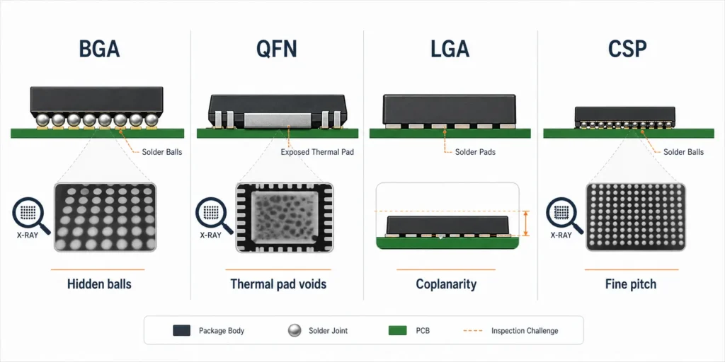
BGA vs QFN, LGA, CSP and Fine-Pitch IC Packages
BGA belongs to a wider group of high-density packages that need tighter assembly control.
| Package type | Assembly concern | Typical inspection concern |
|---|---|---|
| BGA | Solder balls are hidden under the package | X-ray is commonly used for hidden solder joint review |
| CSP | Very small package, often with tight pitch and limited process margin | Fine paste control, placement accuracy, X-ray review |
| LGA | Flat pads under the package, no solder balls on the component | Coplanarity, paste control, hidden joint inspection |
| QFN | Bottom thermal pad and side terminations | Voiding, wetting, solder extrusion, X-ray for thermal pad |
| Fine-pitch QFP | Leads are visible but spacing is tight | AOI is useful, but bridging and placement tolerance matter |
| 0201 / 01005 passives | Very small parts with tight placement tolerance | Tombstoning, skew, insufficient solder, paste consistency |
These packages do not all require the same process. They do share one buyer lesson: when the pitch is tight or the joint is hidden, simple visual inspection is not enough.
Why Engineers Choose BGA Packages
Engineers choose BGA packages because they allow high I/O density in a smaller board area. Compared with many peripheral-lead packages, BGA can reduce routing congestion and support advanced chips that cannot fit practical leaded package formats.
BGA packages are common in:
- processors and SoCs
- FPGAs
- DDR memory
- RF and wireless modules
- high-density communication devices
- embedded computing products
- industrial control electronics
- advanced consumer and IoT electronics
- power-management and mixed-signal modules
BGA can support better routing density, shorter interconnect paths, compact product design, and high pin count. The trade-off is that PCB design, fabrication, assembly, inspection, and testing need to be planned together.
Why BGA Assembly Needs More Process Control
BGA assembly needs more process control because its failure modes are harder to see and often harder to repair. Standard SMT methods may work well for many boards, but BGA and fine-pitch packages reduce the process margin.
Hidden Solder Joints Cannot Be Inspected by Eye
For chip resistors, SOICs, many connectors, and QFP packages, optical inspection can see most of the solder joint. For a BGA, the joint is under the package body.
This creates three practical consequences:
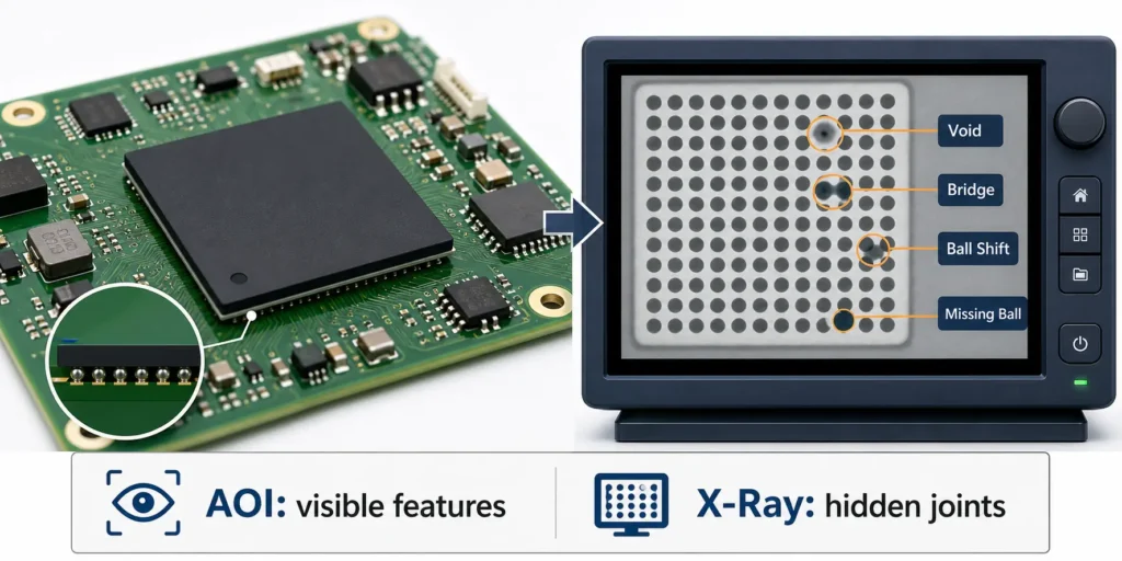
- AOI can confirm package presence, alignment, polarity context, and surrounding visible defects, but it cannot directly see all solder balls.
- Manual visual inspection cannot verify hidden BGA joints.
- X-ray inspection becomes important when the buyer needs evidence of solder bridging, voids, ball shift, missing balls, or abnormal solder distribution.
X-ray is not the whole answer. A BGA joint may look acceptable in X-ray while the board still fails because of a wrong component, firmware issue, poor test access, circuit error, or intermittent functional behavior. Hidden-joint inspection should be paired with electrical and functional testing.
Warpage, Thermal Stress and Solder Joint Reliability
During reflow, the PCB, BGA substrate, solder balls, copper features, and surrounding components expand and contract at different rates. If the BGA package or PCB warps during the liquidus phase, some balls may not wet correctly. The result can be non-wet opens, head-in-pillow defects, intermittent connections, or weak joints.
Warpage risk may be influenced by:
- BGA package size
- PCB thickness
- board size
- copper distribution
- stack-up symmetry
- material selection
- surface finish
- peak reflow temperature
- time above liquidus
- board support during reflow
- cooling behavior
- mechanical stress after assembly
Large BGA packages, thin PCBs, high-density layouts, heavy copper areas, and asymmetric stack-ups deserve careful review before production.
Small Process Variation Can Create Repeated Defects
BGA assembly depends on repeatability. A prototype that works once does not prove that the design is ready for stable pilot production or mass production.
Repeated defects may come from:
- inaccurate land pattern
- solder mask registration issues
- unfilled via-in-pad
- uneven solder paste volume
- stencil aperture problems
- paste aging or poor storage
- BGA moisture exposure
- placement offset
- insufficient PCB support
- poor reflow profile
- X-ray criteria not defined
- test plan discovered too late
DFM and NPI review exist to catch these risks while they are still inexpensive to correct.
BGA DFM Checklist Before Sending an RFQ
A BGA project should be reviewed before the buyer expects a final quote. The supplier needs to know whether the board is manufacturable, assemblable, inspectable, testable, and repairable enough for the intended use.
The DFM review should connect PCB fabrication, SMT assembly, inspection, testing, and final product risk.
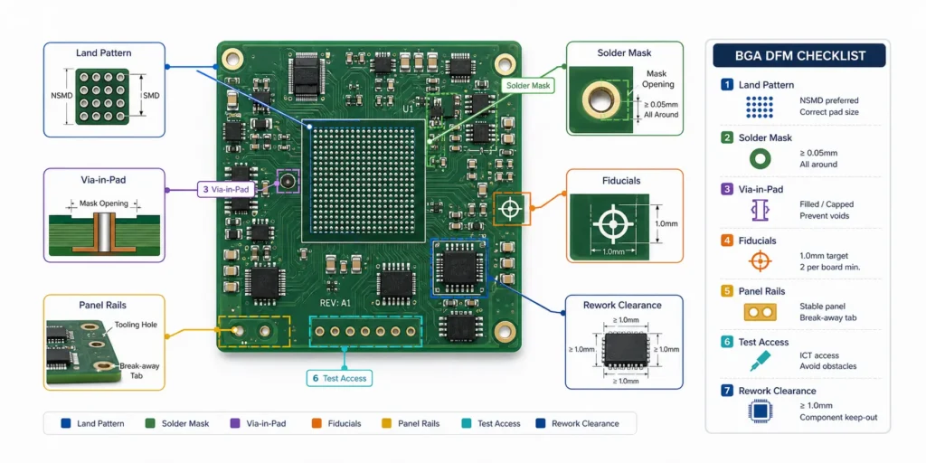
Land Pattern and Solder Mask Design
BGA land pattern design should be checked against the component datasheet, IPC guidance where applicable, PCB fabrication capability, and assembly process requirements. A CAD library footprint is a starting point, not proof that the design is production-ready.
Key items include:
- BGA pitch and ball diameter
- pad diameter
- pad tolerance
- solder mask opening
- solder mask registration capability
- copper balance around the package
- pad-to-via spacing
- surface finish compatibility
- whether NSMD or SMD pads are appropriate
For many fine-pitch BGA designs, non-solder mask defined pads are often used because the copper pad defines the solderable area. Solder mask defined pads may be chosen in some cases for mechanical or design reasons. The right choice depends on package recommendation, PCB capability, reliability target, and supplier review.
No pad style should be treated as universal. Confirm the decision with the component datasheet, PCB fabricator, and assembly supplier.
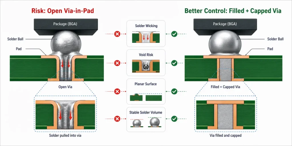
Via-in-Pad, Filled Vias and Escape Routing
Dense BGA fanout often requires via-in-pad or HDI structures. If vias are placed in BGA pads and are not properly filled, capped, or planarized, solder may wick into the via during reflow. That can reduce solder volume at the joint and contribute to voids, opens, or inconsistent ball collapse.
Before quotation, clarify:
- whether via-in-pad is used
- whether vias are filled, capped, or plated over
- whether non-conductive or conductive fill is required
- whether microvias or buried vias are used
- whether the PCB fabricator can meet the via structure
- whether the surface is flat enough for fine-pitch assembly
- whether the design creates solderability or inspection concerns
Via-in-pad is not only a layout decision. It affects fabrication cost, assembly control, and inspection risk.
For related PCB fabrication considerations, see PCBAgroup’s HDI PCB guide.
Fiducials, Panelization and Board Support
Fiducials help the placement machine align the board or panel accurately. They are especially important for BGA-heavy, fine-pitch, or double-sided SMT assemblies.
A BGA DFM review should check:
- global fiducials on the board or panel
- local fiducials near critical fine-pitch components when needed
- fiducial size and clearance
- panel rails
- tooling holes
- V-score or tab routing method
- depanelization stress
- support under large BGA areas during SMT and reflow
Poor panelization can create production risk even when the circuit design is correct. A panel that bends during printing, placement, reflow, or depanelization can create solder joint stress or placement variation.
Component Spacing and Rework Clearance
BGA components should be placed with inspection, rework, and final product assembly in mind. If a BGA is boxed in by tall connectors, shields, heat sinks, transformers, plastic parts, or sensitive components, later rework may be difficult or unsafe.
Review:
- distance from tall components
- access for rework nozzle and thermal shielding
- risk to nearby plastic or heat-sensitive parts
- opposite-side component interference
- X-ray imaging access
- fixture pressure points
- test probe or programming access
- enclosure or mechanical assembly stress
Clearance recommendations vary by package, equipment, board design, and supplier process. The useful buyer takeaway is simple: review rework access before layout release, not after the first failed board.
Standards and Acceptance Criteria Should Be Agreed Early
Buyers may reference IPC-A-610, J-STD-001, IPC-7095, J-STD-033, or customer-specific quality requirements when relevant. Still, one void limit, rework limit, or inspection plan should not be treated as universal for every BGA project.
Before production, align on:
- required IPC class or customer acceptance standard
- whether BGA voiding criteria are defined
- whether X-ray images are required
- whether rework is allowed
- how many rework cycles are acceptable, if any
- whether cross-section, reliability testing, or 3D inspection is required
- what test records must be delivered
This matters most for medical, industrial, telecom, automotive-related, safety-critical, or other high-reliability projects where customer requirements may be stricter than standard commercial electronics.
Stencil, Solder Paste and SPI Control for BGA Assembly
Many BGA defects begin at the solder paste printing stage. Once a BGA is placed, solder volume under the component is difficult to judge directly without X-ray or destructive analysis. Stencil design and SPI therefore become early control points.
Why Stencil Aperture Design Matters
The stencil determines how much solder paste is deposited on each pad. Too much paste may increase bridging, solder balling, or abnormal collapse. Too little paste may create opens, weak joints, or head-in-pillow risk.
Stencil review should consider:
- stencil thickness
- aperture size
- aperture shape
- aperture area ratio
- paste release behavior
- stencil finish
- BGA pitch
- QFN thermal pad segmentation
- coexistence of fine-pitch and large components
- whether a step stencil is needed
In a mixed assembly, the paste volume needed for a fine-pitch BGA may not suit a large connector pad, shield pad, or power component. A step stencil may help when different board areas need different paste volumes. The final choice should be confirmed by the assembly supplier based on component mix and process capability.
Solder Paste Selection and Storage
Solder paste is not just a consumable. Alloy, flux chemistry, powder size, storage, handling, stencil life, and printing behavior can all affect BGA soldering quality.
Items to confirm include:
- lead-free or leaded process requirement
- solder alloy
- no-clean or water-wash chemistry
- powder size suitable for aperture dimensions
- paste storage temperature
- room-temperature recovery before printing
- stencil life
- cleaning frequency
- compatibility with cleaning or coating requirements
The buyer usually does not need to specify every paste parameter unless a customer standard requires it. The buyer should, however, explain the product environment, cleanliness needs, coating needs, and reliability expectations so the supplier can choose a suitable process.
Moisture Sensitivity and Component Handling
Many BGA packages are moisture-sensitive. If a component absorbs moisture and then goes through reflow, internal pressure may cause delamination, cracking, or package damage, often called popcorning.
For BGA and IC packages, buyers and suppliers should check:
- moisture sensitivity level from the datasheet
- whether the original moisture barrier bag is sealed
- humidity indicator card condition
- desiccant condition
- floor life after opening
- baking requirements if floor life is exceeded
- handling of partial reels, trays, or samples
- storage humidity control
Baking requirements vary by package and standard. Follow component documentation, JEDEC-related requirements where applicable, and the supplier’s process control rather than assuming one universal bake condition.
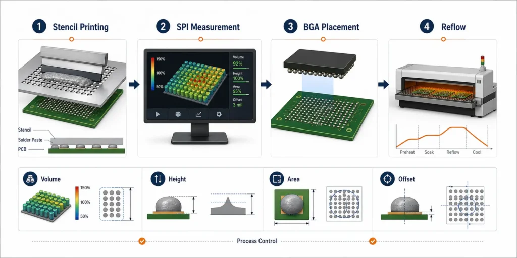
How SPI Helps Prevent Defects Before Placement
Solder paste inspection, or SPI, measures paste deposits after printing and before placement. For BGA and QFN packages, SPI is valuable because it catches printing problems before the defect becomes hidden under a component.
SPI can measure or detect:
- paste volume
- paste height
- paste area
- paste offset
- insufficient paste
- excessive paste
- poor paste shape
- clogged aperture
- stencil alignment drift
- process trend variation
SPI does not guarantee a perfect solder joint after reflow, but it prevents a poor print from moving forward into placement and reflow.
For a broader manufacturing overview, see PCBAgroup’s PCB assembly process guide.
Placement and Reflow Control for BGA Packages
After solder paste printing, placement and reflow become the next major control points. BGA packages need accurate alignment, suitable placement force, stable board support, and a reflow profile matched to the solder paste, PCB thermal mass, package limits, and customer requirements.
Pick-and-Place Accuracy and Vision Alignment
BGA placement depends on machine accuracy, feeder setup, nozzle selection, vacuum control, vision alignment, PCB fiducials, and correct centroid data.
For BGA and fine-pitch packages, the supplier should review:
- package body size
- ball pattern
- placement tolerance
- component orientation
- nozzle contact area
- bottom-vision recognition
- local fiducials if needed
- top and bottom side assembly sequence
- centroid file consistency
- assembly drawing and polarity notes
Buyers can reduce setup risk by providing a complete centroid file with X/Y coordinates, rotation, side, and reference designators. If Gerber, BOM, centroid, and assembly drawing revisions do not match, the supplier has to stop and clarify.
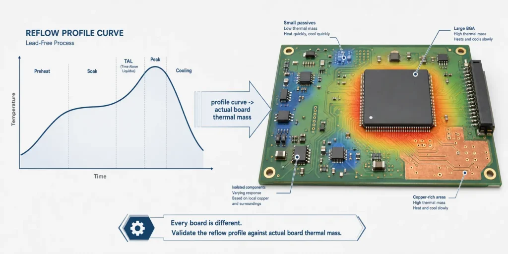
Reflow Profile Control for Mixed Thermal Mass
BGA soldering quality depends heavily on reflow behavior. A suitable profile must heat the board enough for proper wetting while staying within component and PCB limits.
Typical lead-free BGA profile review considers:
- preheat ramp rate
- soak behavior
- flux activation
- time above liquidus
- peak temperature
- temperature difference across the board
- cooling rate
- sensitivity of nearby components
- board warpage risk
Mixed thermal mass makes the job harder. A board may contain a large BGA, small 0201 passives, connectors, shields, power components, and copper planes. These areas heat at different speeds. A profile that works for one area may be too hot, too cold, too fast, or too slow for another.
For high-risk projects, the supplier may validate the profile during NPI using thermocouples at critical locations. The exact method depends on the product and supplier capability.
Nitrogen Reflow and Special Conditions
Some fine-pitch, high-reliability, or difficult-wetting assemblies may benefit from nitrogen reflow or other controlled conditions. Nitrogen can reduce oxidation and improve wetting in selected cases, but it should not be treated as a universal requirement for every BGA assembly.
The need for nitrogen, special flux, special paste, extra cleaning, or extra inspection should be discussed based on:
- package pitch
- surface finish
- solder paste chemistry
- oxidation risk
- customer requirements
- reliability target
- supplier process capability
The practical RFQ question is: “Does this design require any special reflow or process condition beyond your normal SMT process?”
First Article Inspection During NPI
First article inspection confirms that the actual build matches the approved setup before the full batch proceeds.
For BGA assemblies, first article review may include:
- component verification
- placement confirmation
- polarity and orientation check
- SPI result review
- AOI result review
- X-ray review of BGA/QFN devices
- reflow profile confirmation
- electrical test
- functional test
- firmware version check
- test fixture verification
For a new BGA design, first article inspection should not become a paperwork exercise. It is the first serious chance to catch a process or file mismatch before it affects the whole batch.
X-Ray Inspection for BGA Solder Joints
X-ray inspection is central to BGA PCB assembly because it addresses the basic limitation of hidden solder joints. When the joint cannot be seen from outside the package, buyers need another way to evaluate soldering quality.
What X-Ray Inspection Can Detect
Depending on equipment type, image quality, package construction, and operator experience, X-ray inspection can help detect:
- solder bridging
- solder voiding
- ball shift or misalignment
- missing balls
- abnormal solder distribution
- insufficient collapse
- suspected non-wet joints
- solder ball anomalies
- some via-in-pad or pad-related abnormalities
- problems under QFN thermal pads
For BGA, QFN, CSP, LGA, and similar hidden-joint packages, X-ray provides inspection evidence that AOI cannot.
2D X-Ray, AXI and 3D Inspection
Not every X-ray inspection method serves the same purpose.
| Inspection type | Practical use | Buyer note |
|---|---|---|
| Manual 2D X-ray | Common for prototypes, NPI review, selected package inspection | Operator judgment matters |
| Automated X-ray inspection (AXI) | Useful for repeat production and defined inspection programs | Setup and criteria must be agreed |
| 3D X-ray / laminography / CT | Useful for complex overlap, high-reliability review, or detailed analysis | Usually higher cost and should be project-justified |
Buyers do not need to request the most expensive inspection method by default. The right choice depends on product risk, production quantity, package complexity, customer requirements, and supplier capability.
What X-Ray Inspection Cannot Replace
X-ray inspection does not replace every other quality control method.
It does not replace:
- SPI for solder paste control
- AOI for visible component and solder defects
- ICT or flying probe for electrical connectivity
- FCT for real product behavior
- firmware programming verification
- calibration
- burn-in or environmental validation
- root-cause analysis of intermittent failures
X-ray checks hidden solder joint conditions. It does not prove that the final product works in the customer’s application.
When Buyers Should Request X-Ray Inspection
Buyers should discuss X-ray inspection when the assembly includes:
- BGA packages
- QFN packages
- LGA or CSP devices
- high-density assemblies
- fine-pitch ICs
- double-sided SMT with hidden joints
- industrial, medical, telecom, outdoor, or long-life applications
- products where field failure cost is high
The RFQ should state whether X-ray is required for every BGA, selected critical parts, first article only, sample inspection, or every production board. For higher-reliability products, buyers may request 100% inspection, defined sampling, or additional advanced inspection depending on customer requirements and supplier capability.
For related test planning, see PCBAgroup’s article on AOI vs ICT vs FCT in PCBA testing.
Common BGA Assembly Defects and How to Reduce Them
BGA defects can come from design, fabrication, component handling, solder paste printing, placement, reflow, inspection criteria, mechanical stress, or rework. A strong BGA assembly plan looks for the source of risk early instead of waiting for X-ray or FCT failure.
Solder Bridging and Insufficient Solder
Solder bridging occurs when solder connects adjacent joints that should remain separate. Insufficient solder occurs when the joint lacks enough solder volume or wetting.
Possible causes include:
- excessive paste
- insufficient paste
- poor stencil aperture design
- stencil wear or contamination
- solder mask registration issue
- placement offset
- package or PCB warpage
- improper reflow behavior
Risk reduction may include:
- reviewing land pattern and solder mask
- optimizing stencil aperture design
- using SPI to monitor paste deposits
- maintaining stencil cleaning control
- validating placement alignment
- reviewing reflow profile
- using X-ray to verify hidden joints
Voids Under BGA Solder Balls
Voids are gas pockets inside solder joints. Some voiding may occur in many soldering processes, but excessive voiding or voids in critical locations may affect thermal, electrical, or mechanical reliability depending on product use.
Void risk may be influenced by:
- solder paste chemistry
- reflow profile
- pad design
- via-in-pad quality
- PCB finish
- PCB or component moisture
- flux outgassing
- contamination
- QFN thermal pad design
Avoid writing one universal void percentage into the RFQ unless the customer or standard requires it. A better approach is to ask the supplier to confirm acceptance criteria based on package type, product risk, customer standard, and inspection capability.
Head-in-Pillow and Non-Wet Opens
Head-in-pillow occurs when the solder ball and paste appear to contact but do not fully merge into one reliable joint. Non-wet opens may create complete or intermittent failures.
Possible causes include:
- BGA package warpage
- PCB warpage
- oxidation on ball or pad
- insufficient paste
- paste degradation
- poor moisture control
- reflow profile mismatch
- thermal imbalance
Prevention depends on component handling, pad solderability, paste control, reflow validation, and package warpage awareness. This is why high-risk BGA projects deserve NPI review rather than routine SMT handling.
Pad Cratering and Mechanical Stress
Pad cratering is damage in the PCB laminate under a pad. It may occur because of bending, shock, connector insertion, depanelization, fixture pressure, or repeated mechanical stress.
Risk reduction may involve:
- avoiding BGA placement near board edges or high-stress zones
- reviewing depanelization design
- supporting the PCB during test and assembly
- controlling connector insertion stress
- reviewing fixture contact points
- considering mechanical reinforcement when required
- defining handling rules for large or thin boards
Pad cratering is often not solved by X-ray alone. Depending on the case, it may require design review, mechanical analysis, cross-section, or failure analysis.
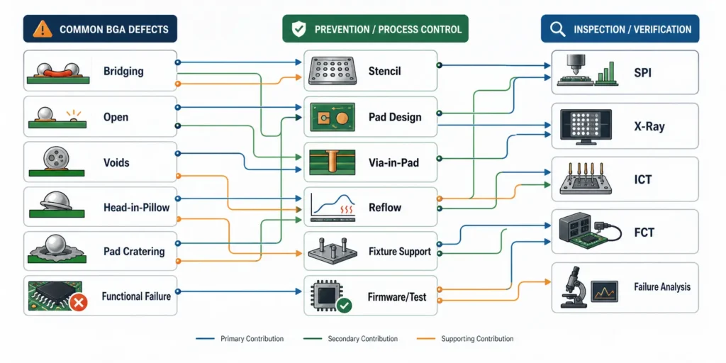
BGA Failure Prevention Map
| Failure mode | Early prevention point | Inspection or validation method |
|---|---|---|
| Bridging | Stencil, paste volume, placement alignment | SPI, X-ray, electrical test |
| Opens | Pad design, paste volume, warpage control | X-ray, ICT, FCT |
| Voiding | Via-in-pad, paste, reflow, moisture | X-ray, process review |
| Head-in-pillow | Package handling, warpage, reflow | X-ray, electrical/functional test |
| Pad cratering | Layout, depanelization, fixture support | Mechanical review, failure analysis |
| Functional failure | Test access, firmware, component correctness | ICT, FCT, programming verification |
This table shows why one inspection method cannot cover every BGA risk.
Testing Strategy for BGA PCB Assemblies
A BGA assembly can pass X-ray and still fail in function. It can pass FCT and still hide process variation that matters in repeat production. The test strategy should match product risk and project stage.
SPI, AOI, X-Ray, ICT and FCT Roles
| Test or inspection | What it detects | Where it fits |
|---|---|---|
| SPI | Solder paste volume, height, area, offset | Post-print, before placement |
| AOI | Component presence, polarity, visible solder defects, tombstoning | Post-reflow for visible features |
| X-ray | Hidden solder joints under BGA/QFN/CSP/LGA, voids, bridging, ball shift | Post-reflow for hidden joints |
| Flying probe | Electrical opens/shorts without fixture | Prototype, NPI, low volume, changing designs |
| ICT | Electrical values, shorts, opens, power rail checks with fixture | Repeat production where test access supports it |
| FCT | System-level function, firmware boot, I/O behavior, customer-defined operation | Final validation stage |
| Burn-in / reliability testing | Operation under defined stress condition | Selected higher-risk products |
These methods are complementary, not interchangeable. A board can pass X-ray but fail ICT because of an electrical issue. It can pass ICT but fail FCT because firmware, communication, calibration, or real operating behavior is wrong.
Firmware, Programming and Pass/Fail Criteria
Many BGA-based assemblies include processors, memory, wireless modules, FPGAs, or programmable devices. If firmware is involved, the buyer should provide test information before production.
Useful information includes:
- firmware file
- firmware version
- programming interface
- programming tool requirements
- checksum or CRC verification
- boot sequence
- self-test procedure
- communication protocol
- voltage and current limits
- load condition
- calibration steps
- pass/fail criteria
- expected test report format
Without these details, the supplier may be able to assemble the board but may not be able to prove that it performs correctly.
Test Records and Traceability
For higher-reliability BGA assemblies, buyers may need records for quality review, audits, repeat production, or failure analysis.
Useful records may include:
- first article inspection result
- SPI report or trend summary
- AOI result
- X-ray image or inspection summary
- ICT or flying probe result
- FCT log
- firmware version record
- serial number or lot traceability
- rework record
- final inspection report
Not every project needs every record. The buyer should define required documentation during RFQ review, because collecting and storing records affects cost, lead time, and process flow.
BGA Rework: When It Is Possible and When It Is Risky
BGA rework is sometimes possible, but it should not be the main production strategy. Rework requires controlled heating, skilled operators, suitable equipment, and follow-up inspection. It also exposes the PCB and nearby components to additional thermal stress.
Typical BGA Rework Process
A typical BGA rework process may include:
- Confirming the suspected defect through X-ray, ICT, FCT, or failure analysis
- Protecting nearby heat-sensitive components
- Preheating the PCB to reduce localized thermal stress
- Removing the BGA with controlled hot air or IR equipment
- Cleaning residual solder from the PCB pads
- Inspecting pad condition and solder mask condition
- Preparing a replacement component or reballed component
- Aligning the BGA with suitable vision support
- Reflowing the replacement component
- Inspecting the reworked area with X-ray
- Running electrical or functional test again
The exact process depends on package size, board thickness, component availability, coating, nearby parts, and defect condition.
Risks of Repeated BGA Rework
Repeated rework may cause:
- pad lifting
- pad cratering
- solder mask damage
- laminate stress
- nearby component damage
- local board warpage
- flux residue risk
- increased intermetallic growth
- reduced reliability of the repaired area
- longer test and inspection time
Some projects may allow limited BGA rework. Others may restrict rework or require customer approval. This should be defined before production, especially for high-reliability assemblies.
Why Prevention Is Better Than Repair
Prevention usually costs less than repair because it avoids:
- engineering clarification after failure
- line stoppage
- X-ray retest
- component replacement
- rework labor
- scrap risk
- schedule delay
- customer approval delay
- shipment uncertainty
For BGA assembly, prevention means early DFM review, stable solder paste printing, SPI, accurate placement, validated reflow, suitable X-ray inspection, clear test criteria, and controlled component handling.
BGA Assembly Cost and Lead Time Drivers
BGA assembly cost is not determined only by component count. A board with one difficult BGA may require more engineering review than a larger board with only standard passive components and connectors.
Cost and lead time depend on how much risk must be controlled.
What Increases BGA Assembly Cost
Common cost drivers include:
- number of BGA, QFN, CSP, and LGA packages
- fine pitch
- high ball count
- PCB layer count
- HDI and microvia structure
- via-in-pad filling and capping
- surface finish
- stencil complexity
- double-sided SMT
- X-ray inspection scope
- first article inspection
- ICT or FCT fixture design
- firmware programming setup
- rework risk
- low-volume NRE
- documentation and traceability
- special processes such as cleaning or conformal coating
A low assembly price may not be the lowest total cost if it excludes inspection, testing, engineering review, fixture planning, or documentation needed to control the project.
Prototype vs Production Cost Behavior
| Stage | Cost behavior | Main decision |
|---|---|---|
| Prototype | Higher setup cost per board, more engineering questions, flexible testing | Learn whether design and process risks exist |
| Pilot run | Process review, first article, yield observation, test planning | Decide whether the design is ready to scale |
| Mass production | Fixture amortization, repeatability, sourcing stability, inspection records | Control quality, cycle time, and field risk |
For prototypes, 100% X-ray review or deeper inspection may be justified for learning. For production, the buyer and supplier may agree on 100% inspection, defined sampling, AXI, or other criteria depending on product risk and process maturity.
How to Avoid Late Quotation Changes
Late quotation changes usually happen when requirements appear after the supplier has already quoted.
Avoid vague RFQ wording such as:
- “standard inspection”
- “normal test”
- “high quality”
- “X-ray if needed”
- “supplier decide”
Use clearer wording:
This assembly includes BGA, QFN, and fine-pitch components. Please review DFM before quotation, including land pattern, via-in-pad, solder mask, stencil, reflow, X-ray inspection, rework access, and test requirements. Please quote X-ray inspection, functional testing, programming, fixture cost, and any NRE separately where applicable.
This gives engineering and procurement teams a better basis for comparing suppliers.
BGA PCB Assembly RFQ Checklist
A strong BGA PCB assembly RFQ reduces assumptions. The supplier should understand what is being built, which parts are high-risk, what inspection is expected, what testing is required, and what records must be delivered.
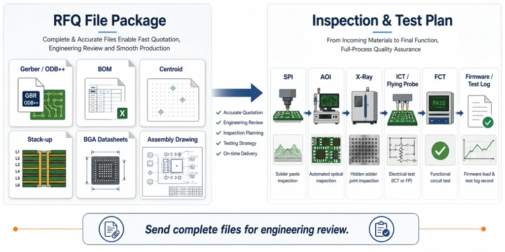
Files Buyers Should Provide
| File | Purpose |
|---|---|
| Gerber or ODB++ | PCB fabrication and assembly review |
| NC drill and drill map | Hole and via review |
| PCB stack-up | Material, thickness, copper, impedance, and warpage review |
| BOM with MPNs | Sourcing and package identification |
| Centroid / pick-and-place file | SMT programming and placement review |
| Assembly drawing | Orientation, polarity, mechanical notes |
| BGA datasheets | Package pitch, ball map, MSL, land pattern, reflow guidance |
| Fabrication drawing | Surface finish, tolerances, via filling, controlled impedance |
| Test procedure | ICT, flying probe, FCT, programming, calibration |
| Firmware file | Programming and version control |
| Approved alternates list | Component substitution control |
| Quality requirements | IPC class, reports, traceability, X-ray, rework limits |
For general RFQ preparation, see PCBAgroup’s PCBA RFQ package checklist.
Requirements Buyers Should Specify
Specify:
- BGA/QFN/LGA/CSP list
- package pitch and body size if known
- via-in-pad locations and treatment
- surface finish requirement
- IPC class or customer acceptance criteria
- X-ray inspection scope
- 2D, AXI, or advanced inspection need if required
- ICT, flying probe, FCT, or programming requirement
- firmware version and pass/fail criteria
- quantity and forecast
- target delivery schedule
- report and traceability requirements
- rework policy
- packaging and labeling needs
- product application and operating environment
The goal is not to overload the supplier. The goal is to prevent hidden assumptions that later affect cost, quality, and schedule.
Questions to Ask a BGA Assembly Supplier
Before choosing a supplier for BGA PCB assembly, ask:
- What BGA pitch and package types do you regularly support?
- Can you review BGA footprint, solder mask, via-in-pad, and stencil risk before quotation?
- Do you use SPI for BGA or fine-pitch paste inspection?
- Do you provide X-ray inspection for BGA or hidden-joint packages?
- Can you share X-ray images or inspection summaries if required?
- How do you define and handle BGA voiding concerns?
- What is your first article inspection process for new BGA designs?
- Can you support FCT, programming, or customer-defined testing?
- What information do you need for a test fixture?
- How do you control Gerber, BOM, centroid, and firmware revision matching?
- How is BGA rework approved and documented?
- What production records can be provided for repeat orders?
These questions help buyers evaluate real engineering support rather than only comparing unit price.
How PCBAgroup Supports BGA and Fine-Pitch PCB Assembly
PCBAgroup’s public service pages describe PCB assembly and PCB fabrication support, including SMT assembly, through-hole assembly, mixed assembly, turnkey/consigned/partial-turnkey sourcing, SPI, AOI, X-ray inspection, first article inspection, and MES-related quality control. Public service content also lists small passive component assembly such as 01005/0201/0402, BGA handling with X-ray testing, and fine-pitch assembly capability.
These are useful capability signals for buyers with BGA, QFN, fine-pitch, or high-density PCB assembly projects. The final process should still be confirmed project by project.
Published Assembly Capability Signals
For BGA and fine-pitch projects, buyers should pay attention to:
- SMT assembly capability
- small passive component handling
- BGA and fine-pitch package handling
- SPI for solder paste inspection
- AOI for visible assembly inspection
- X-ray for hidden solder joint review
- first article inspection
- functional testing support where required
- MES-related traceability
- component sourcing model
Confirm the exact inspection scope, pitch support, X-ray coverage, test responsibility, report format, and rework policy before production.
Engineering Review Before Production
For BGA PCB assembly, early engineering review should connect:
- PCB fabrication requirements
- BGA package data
- footprint and solder mask
- via-in-pad treatment
- stencil and paste strategy
- component sourcing and MSL handling
- SMT process flow
- X-ray inspection plan
- firmware and functional test plan
- rework policy
- documentation and traceability
A useful BGA assembly quote should clarify assumptions. If a quote gives only unit price and lead time but ignores X-ray, test, rework, via-in-pad, and functional validation, buyers should ask more questions before placing the order.
Suggested RFQ Message for BGA Assembly
Buyers can use wording like this:
This PCBA includes BGA/QFN/fine-pitch components and is intended for prototype/pilot/mass production. Please review the Gerber/ODB++, BOM, centroid file, assembly drawing, BGA datasheets, stack-up, via-in-pad design, surface finish, and test requirements before quotation. Confirm whether the footprint, stencil design, reflow process, X-ray inspection, rework access, programming, and FCT plan are suitable. Please quote PCB fabrication, component sourcing, SMT assembly, X-ray inspection, functional testing, programming, fixture cost, and NRE separately where applicable.
This request gives the supplier enough context to provide engineering feedback, not just a price.
FAQ
Is X-ray inspection required for every BGA PCB assembly?
X-ray inspection is strongly recommended for many BGA assemblies because the solder joints are hidden under the package. Whether every board needs X-ray depends on product risk, volume, customer requirements, and acceptance criteria. For prototypes and high-risk products, buyers often request more complete X-ray review. For stable production, sampling or automated inspection may be agreed if the process is validated.
Can AOI inspect BGA solder joints?
AOI can inspect visible features such as component presence, placement, polarity context, and surrounding visible solder defects. It cannot directly inspect all solder balls hidden under a BGA package. For hidden joints, X-ray inspection is usually the more relevant inspection method.
What files are needed for a BGA PCB assembly quote?
A useful BGA assembly RFQ should include Gerber or ODB++ files, BOM with MPNs, centroid file, assembly drawing, PCB stack-up, BGA datasheets, surface finish requirement, via-in-pad notes, test requirements, X-ray expectations, quantity, target schedule, and any quality or traceability requirements.
What causes BGA solder voids?
BGA solder voids may be caused by solder paste chemistry, outgassing, reflow profile, pad design, via-in-pad condition, PCB finish, contamination, or moisture in the PCB or component package. The acceptable void level should be defined according to product risk, customer requirements, package type, and inspection capability rather than guessed after production.
Can BGA components be reworked?
Many BGA components can be reworked with proper equipment and process control. The process may include removal, pad cleaning, replacement or reballing, controlled local reflow, X-ray inspection, and functional retesting. However, BGA rework is slower and riskier than preventing the defect. Rework limits should be agreed before production for high-reliability products.
Why is BGA assembly more expensive than standard SMT?
BGA assembly may cost more because it can require deeper DFM review, controlled stencil design, SPI, precise placement, X-ray inspection, special component handling, rework planning, functional testing, fixtures, and documentation. The cost depends on package pitch, board complexity, inspection scope, quantity, and test requirements.
Should I involve the PCBA supplier before PCB layout is finished?
Yes, if the design includes fine-pitch BGA, via-in-pad, HDI routing, double-sided SMT, high-density placement, special testing, or reliability-sensitive applications. Early supplier feedback can help prevent footprint, routing, panelization, test access, and rework problems before the layout is locked.
What is the difference between BGA, QFN and CSP in assembly risk?
BGA uses solder balls under the component body. QFN uses bottom pads and often a thermal pad. CSP is a very compact package, often with tight pitch and limited process margin. They differ in structure, but all may create inspection and process-control challenges because some or all solder joints are hidden or tightly spaced.
Does BGA assembly always require ICT or FCT?
Not always. X-ray inspection checks hidden solder joint conditions, but it does not prove full product function. ICT, flying probe, boundary scan, or FCT may be needed depending on circuit complexity, test access, volume, firmware, and customer requirements. For many high-value assemblies, X-ray plus functional testing gives better risk control than either method alone.
Conclusion: Treat BGA Assembly as an Engineering Review, Not Only a Placement Job
BGA PCB assembly can be reliable and efficient when the design, process, inspection, and test plan are aligned early. The main risk is not the BGA package itself. The main risk is treating hidden-joint, high-density assembly like a simple SMT order.
For engineers, the priority is to review footprint, solder mask, via-in-pad, surface finish, spacing, panelization, test access, and rework clearance before the design is locked.
For procurement teams, the priority is to compare suppliers by engineering review quality, process capability, X-ray inspection, testing support, documentation, traceability, and communication clarity, not only by unit price.
If your project includes BGA, QFN, LGA, CSP, fine-pitch components, HDI routing, firmware programming, or reliability-sensitive use conditions, prepare a complete file package before quotation. A clear RFQ gives the PCBA manufacturer enough information to review the design, control the assembly process, inspect hidden joints, plan testing, and reduce avoidable production risk.
To request a BGA PCB assembly review, prepare your Gerber or ODB++ files, BOM, centroid file, assembly drawing, BGA datasheets, PCB stack-up, quantity, target schedule, X-ray requirements, firmware notes, and test plan. PCBAgroup can review the project requirements and help identify the manufacturing, inspection, testing, and documentation items that should be confirmed before production.